EasyManua.ls Logo

Allwinner A20 - PS2 Block Diagram; PS2 Timing Diagram

Allwinner A20
812 pages
Print Icon
To Next Page IconTo Next Page
To Previous Page IconTo Previous Page
Loading...
A20 User Manual (Revision 1.2) Copyright © 2013 Allwinner Technology Co., Ltd. All Rights Reserved. Page 631 / 812
6.5.2. PS2 Block Diagram
APB Interface
&
Register Block
PCLK
PSEL
PWRITE
PENABLE
PADDR[9:0]
PWDATA[31:0]
PRDATA[31:0]
PRESETn
IRQ
Transmit
Engine
Receive
Engine
TXFIFO
RXFIFO
PS2_DATA_OUT
PS2_DATA_OE
PS2_DATA_IN
Sample
Divider
PS/2 CLOCK
Controller
PS2_CLK_OUT
PS2_CLK_OE
PS2_CLK_IN
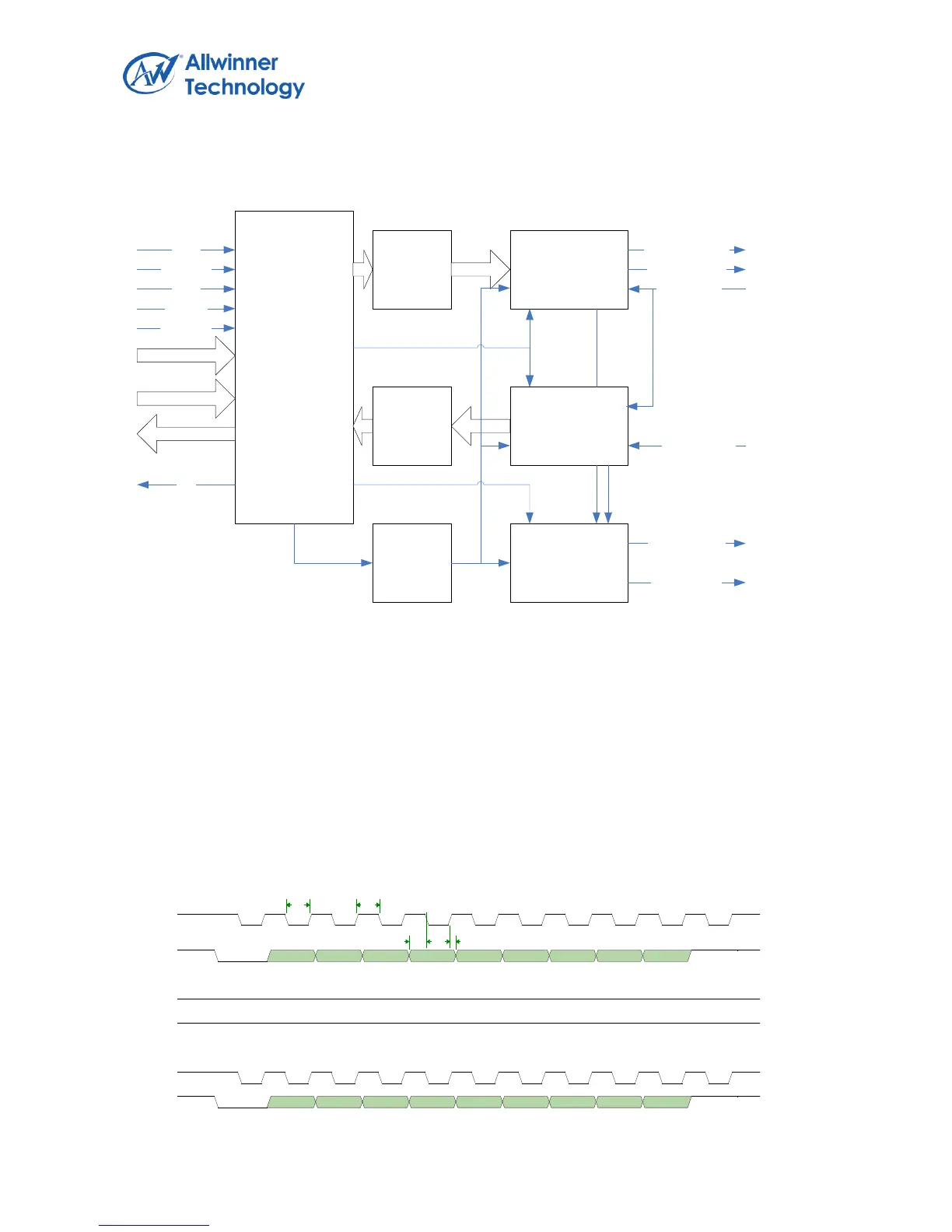
6.5.3. PS2 Timing Diagram
The Data and Clock lines of PS2 Bus are both open-collector with pull-up resistors to power, and so,
Data and Clock signals on PS2 Bus are both wire-and by corresponding signal of Host and Device.
Data is transferred after start bit, starting with the least significant bit(LSB). These are followed by the
parity bit, followed by one stop bit. If data is transferred from master to device, there is an additional
acknowledge bit(ACK) sent by device, following the stop bit.
Timing for Device Transmit Data and Master Receive Data:
STA
D0
D1
D2
D3
D4
D5
D6
D7
PAR
STP
STA
D0
D1
D2
D3
D4
D5
D6
D7
PAR
STP
Tr2dTd2f
TckhTckhTcklTckl
CLOCK
DATA
HOST_CLOCK
HOST_DATA
DEVICE_CLOCK
DEVICE_DATA

Table of Contents