A20 User Manual (Revision 1.2) Copyright © 2013 Allwinner Technology Co., Ltd. All Rights Reserved. Page 61 / 812
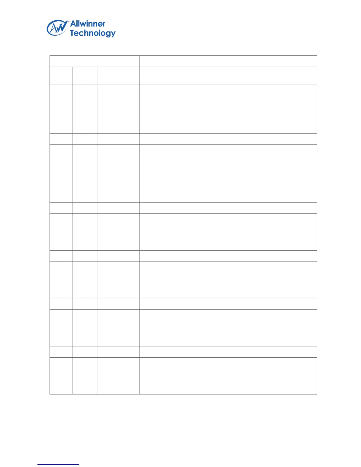
Register Name: SD2_CLK_REG
SCLK_GATING.
Gating Special Clock(Max Clock = 200MHz)
0: Clock is OFF
1: Clock is ON
This special clock = Clock Source/Divider N/Divider M.
CLK_SRC_SEL.
Clock Source Select
00: OSC24M
01: PLL6
10: PLL5
11: /.
CLK_PHASE_CTR.
Sample Clock Phase Control.
The sample clock phase delay is based on the number of
source clock that is from 0 to 7.
CLK_DIV_RATIO_N.
Clock pre-divide ratio (n)
The select clock source is pre-divided by 2^n. The divider is
1/2/4/8.
OUTPUT_CLK_PHASE_CTR.
Output Clock Phase Control.
The output clock phase delay is based on the number of source
clock that is from 0 to 7.
CLK_DIV_RATIO_M.
Clock divide ratio (m)
The pre-divided clock is divided by (m+1). The divider is from 1
to 16.