System Control
ARM DDI 0500D Copyright © 2013-2014 ARM. All rights reserved. 4-156
ID021414 Non-Confidential
4.4.28 AArch32 Implementation defined registers
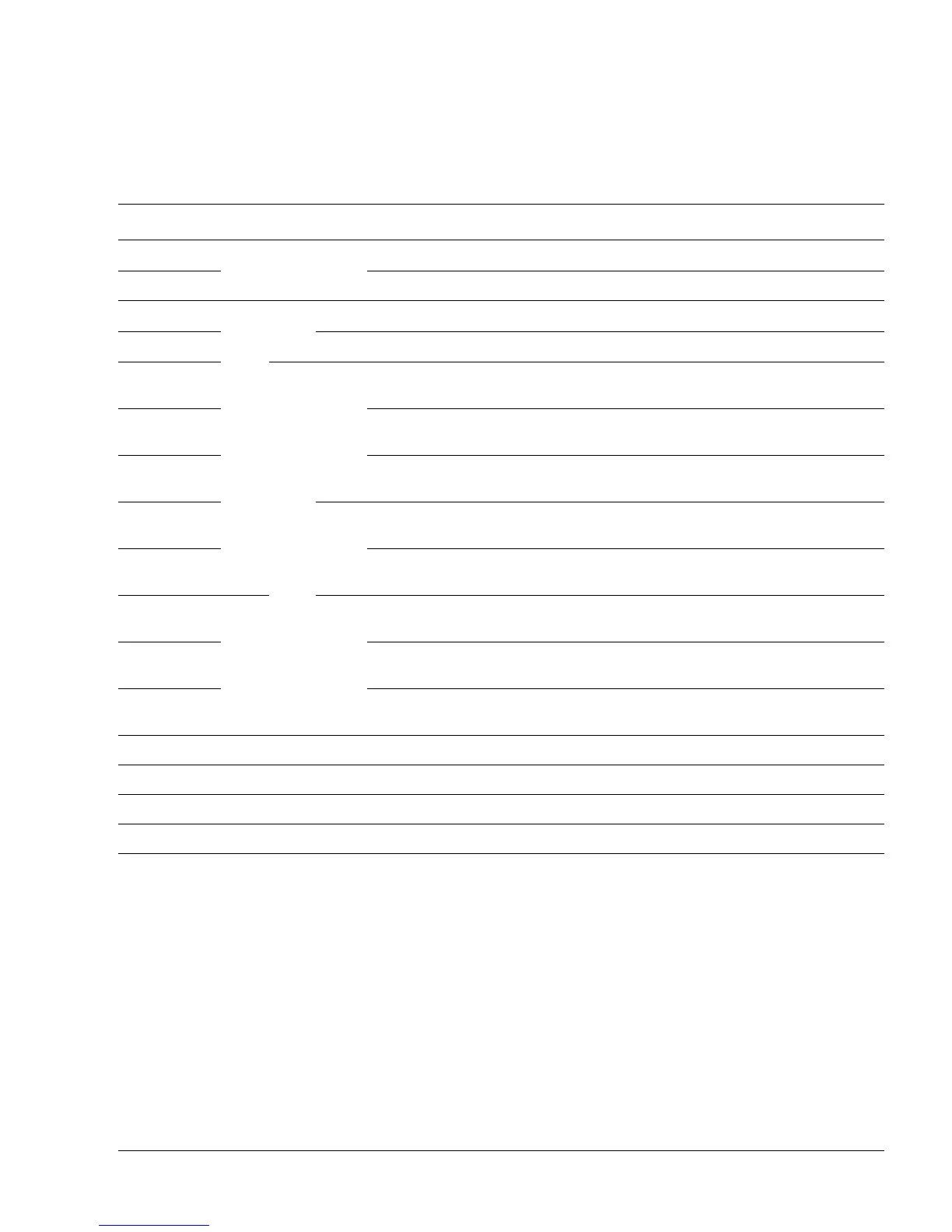
Table 4-147 shows the 32-bit wide implementation defined registers. These registers provide
test features and any required configuration options specific to the Cortex-A53 processor.
Table 4-147 Memory access registers
Name CRn Op1 CRm Op2 Reset Description
L2CTLR c9 1 c0 2
-
a
L2 Control Register on page 4-251
L2ECTLR 3
0x00000000
L2 Extended Control Register on page 4-253
L2ACTLR c15 1 c0 0
0x80000000
b
L2 Auxiliary Control Register on page 4-267
CBAR c3 0
-
a
Configuration Base Address Register on page 4-278
CDBGDR0
3
c
c0 0 UNK Data Register 0, see Direct access to internal memory on
page 6-13
CDBGDR1 1 UNK Data Register 1, see Direct access to internal memory on
page 6-13
CDBGDR2 2 UNK Data Register 2, see Direct access to internal memory on
page 6-13
CDBGDCT c2 0 UNK Data Cache Tag Read Operation Register, see Direct
access to internal memory on page 6-13
CDBGICT 1 UNK Instruction Cache Tag Read Operation Register, see
Direct access to internal memory on page 6-13
CDBGDCD c4 0 UNK Data Cache Data Read Operation Register, see Direct
access to internal memory on page 6-13
CDBGICD c4 1 UNK Instruction Cache Data Read Operation Register, see
Direct access to internal memory on page 6-13
CDBGTD 2 UNK TLB Data Read Operation Register, see Direct access to
internal memory on page 6-13
CPUACTLR - 0 c15 -
0x00000000004C8000
CPU Auxiliary Control Register on page 4-269
CPUECTLR - 1 c15 -
0x0000000000000000
CPU Extended Control Register on page 4-271
CPUMERRSR - 2 c15 - - CPU Memory Error Syndrome Register on page 4-273
L2MERRSR - 3 c15 - - L2 Memory Error Syndrome Register on page 4-276
a. The reset value depends on the processor configuration.
b. This is the reset value for an ACE interface. For a CHI interface the reset value is
0x80004008
.
c. See Direct access to internal memory on page 6-13 for information on how these registers are used.