Communication Processor Module
MOTOROLA MPC823e REFERENCE MANUAL 16-105
IDMA
COMMUNICATION
16
PROCESSOR MODULE
16.6.3.11.4 Single-Buffer Burst Fly-By Mode. This mode is used to transfer a data block
from a peripheral to system memory. When the buffer has been completely transferred,
channel operation is terminated. Both progressive (non-interlaced) and interlaced
destination address generation modes are supported. This mode of operation is a subset of
the buffer chaining mode with reduced latency and it is restricted to fly-by transfers. It is
supported only on IDMA channel 1.
Progressive address generation mode is selected by setting the EIE bit in the RCCR, which
is described in Section 16.2.5 RISC Configuration and Control Registers. As a result,
the organization of its parameter RAM is different from the other modes.
Interlaced address generation mode supports charge-coupled devices (CCDs), which use
an interlaced readout scheme and are often used in digital cameras. The frame buffer in
memory must be progressive to decrease the amount of processing the software has to
perform. The interlace mode allows you to read an interlaced CCD into a progressive buffer.
For example, for a 2-field CCD, the IDMA reads a line, skips a line, reads a line until the first
field (the odd lines) is read. Then the process repeats for the second field (even lines). There
are, however, 4-field CCDs, in which case you would read a line and then skip three. A field
is a group of scan lines (odd or even) and a frame is composed of several fields. The refresh
(of the display) or readout (of the CCD) is done by field sequence—field1, then field2, etc.
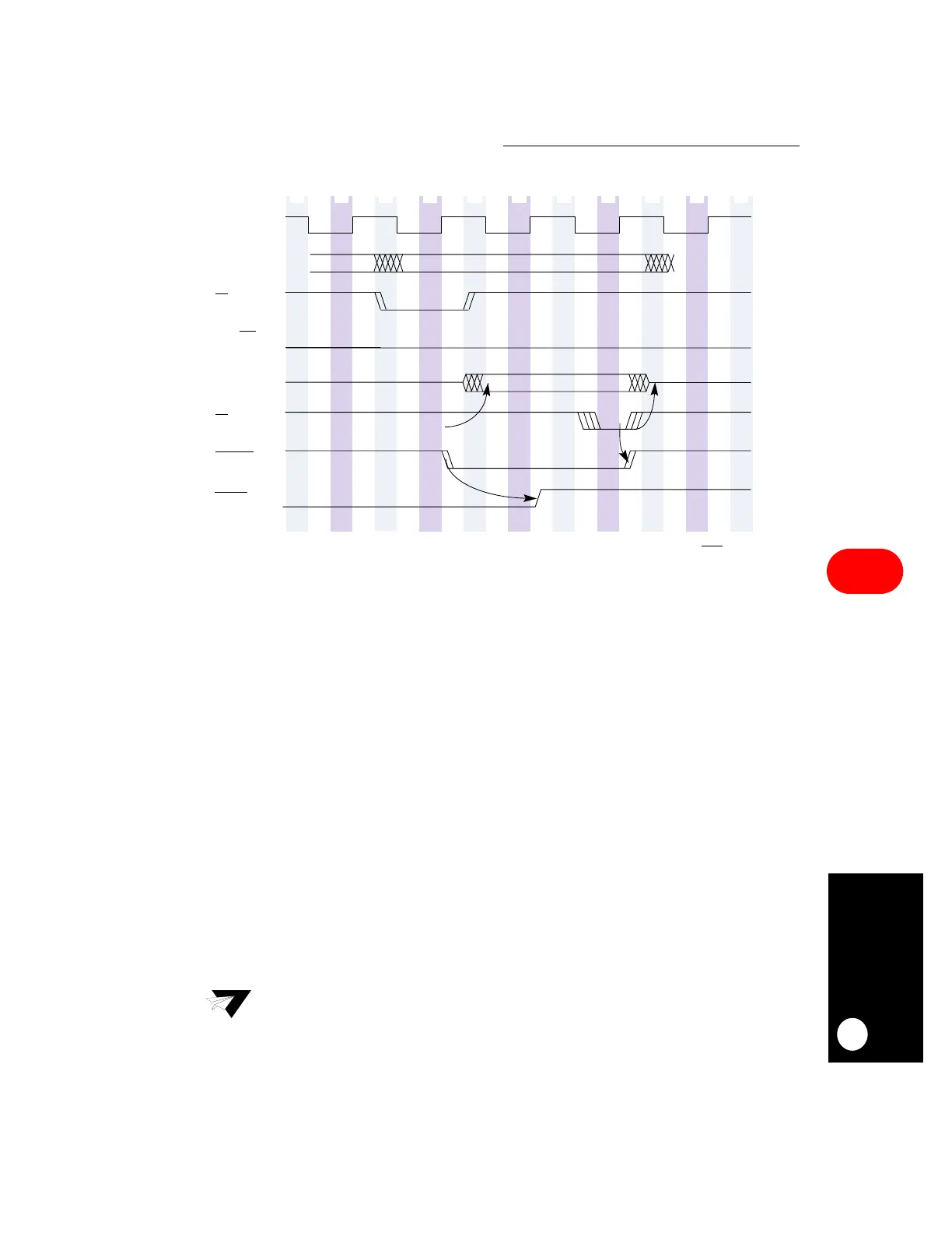
Figure 16-41. Single-Address, Peripheral Read, Synchronous TA
Note: The ARM IDMA command only works with IDMA modes that use buffer
descriptors.
T3T1T3T1T3
CLKOUT
T1 T3 T1 T3 T1 T3
ADDRESS
RD /
WR
TS
DATA
TA
SDACKx
T0 T2 T0
DREQx
 Loading...

