Communication Processor Module
16-106 MPC823e REFERENCEMANUAL MOTOROLA
IDMA
COMMUNICATION
16
PROCESSOR MODULE
Interlaced mode can be set up using the following steps:
1. Initialize the IDMA single buffer mode parameter RAM.
2. In the RCCR, set the EIE bit to 1 and the DR1M bit according to the requested mode.
See Section 16.2.5 RISC Configuration and Control Registers for more
information.
3. If edge-sensitive mode is selected, program the EDM15 bit of the PCINT register to
the requested mode (falling edge/any edge).
4. In the PCSO register, set the DREQ1 bit to 1. See Section 16.14.9.4 Port C Special
Options Register for more information.
When configured to single buffer mode, the IDMA parameter RAM is overlayed with the
specific parameters in Table 16-22.
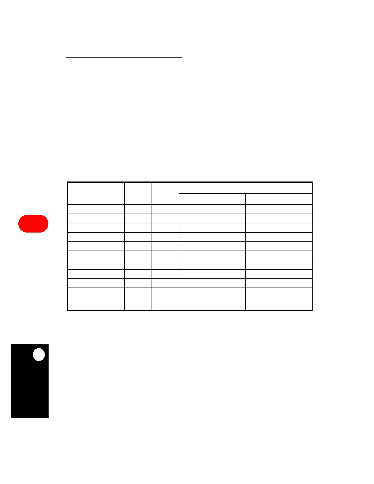
Table 16-22. Single-Buffer Mode Parameter RAM Map
ADDRESS NAME WIDTH
DESTINATION ADDRESS GENERATION MODE
PROGRESSIVE INTERLACED
DMA Base + 00 BAPR* Word Buffer Address Pointer Current Buffer Address Pointer
DMA Base + 04 BCR* Word Byte Count Register Current Bytes Per Line
DMA Base + 08 DCMR* Word DMA Channel Mode Register DMA Channel Mode Register
DMA Base + 0C FBAR* Word Not Assigned Field Base Address Register
DMA Base + 10 RES Half-Word Reserved Reserved
DMA Base + 12 NFLD* Half-Word Not Assigned Number of Fields Register
DMA Base + 14 LCR Half-Word Not Assigned Lines Per Field Count Register
DMA Base + 16 L_CNT* Half-Word Not Assigned Current Line Count
DMA Base + 18 BPLR Half-Word Not Assigned Bytes Per Line Register
DMA Base + 1A RBR Half-Word Not Assigned Raw Bytes Register
DMA Base + 1C to
DMA Base + 3F
RES Word Reserved Reserved
NOTE: You are only responsible for initializing the items in bold.
* Modified by the IDMA controller during operation and must be reinitialized before starting a
new IDMA transaction.
DMA base = (IMMR & 0xFFFF0000) + 0x3CC0 (IDMA1).
All references to registers in the parameter RAM table are actually implemented in the dual-port RAM area as
a memory-based register.