Chapter 9
16-bit Timer
IX - 20 Control registers
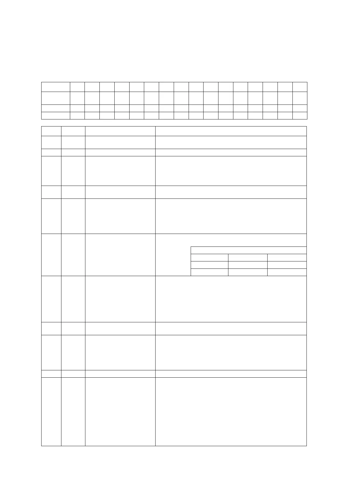
■ Timer 8 Mode Register (TM8MD: 0x0000A200) [8, 16-bit Access Register]
bp 15 14 13 12 11 10 9 8 7 6 5 4 3 2 1 0
Flag TM
XF
-TM
TGE
TM
ONE
TM
CLE
TM
CGE
TM
UD1
TM
UD0
TM
CNE
TM
LDE
---TM
CK2
TM
CK1
TM
CK0
At reset 0000100000000000
Access R R R/W R/W R/W R/W R/W R/W R/W R/W R R R R/W R/W R/W
bp Flag Description Setting condition
15 TMXF
Timer operation display 0: Timer stopped
1: Timer operating
14 - - -
13 TMTGE
Timer external trigger enable 0: Timer activation disabled by external trigger. (trigger input ignored)
1: Timer start when the falling edge is input
(when timer A pin polarity selection bit is “0”)
Timer start when the rising edge is input
(when timer A pin polarity selection bit is “1”)
12 TMONE
Timer 1-shot operation enable 0: 1-shot operation disabled (timer does not stop)
1: 1-shot operation enabled (timer stops when TMBC and TMCA match)
11 TMCLE
Timer binary counter enable 0: Clear operation disabled
1: Clear operation enabled
When the TMCA is set to a compare register
TMBC is cleared when the TMBC and the TMCA match.
When the TMCA is set to a capture register
TMBC is cleared when captured to TMCA.
10 TMCGE
Timer count control input enable 0: Count control disabled by the TMAIN pin input
1: Refer to the following table.
Timer A pin polarity selection bit
TMAIN pin input "0" "1"
"L" Stop counting Counting
"H" Counting Stop counting
9-8
TMUD1
TMUD0
Up/down counting selection 00: Up counting
01: Down counting
10: Up counting (when “H” level is input to the TMAIN pin)
Down counting (when “L” level is input the TMAIN pin)
11: Up counting (when “L” level is input the TMAIN pin)
Down counting (when “H” level is input to the TMAIN pin)
When the 2-phase encoding (1-fold, 4-fold) is selected as the count clock
source, set “00”.
7 TMCNE
Timer operation enable 0: Operation disabled
1: Operation enabled
6TMLDE
Timer initialization 0: Normal operation
1: Initialization
TMBC=0x0000
When the TMCA and TMCB are set to the compare register of the double
buffer, the value is loaded into the compare register from the buffer. Pin out-
put is initialized.
5-3 - - -
2-0
TMCK2
TMCK1
TMCK0
Timer count clock source selection 000: IOCLK
001: IOCLK/8
010: IOCLK/64
011: Timer 2 underflow
100: 2-phase encoding (1-fold)
101: 2-phase encoding (4-fold)
110: TMBIN pin input (both edges)
111: TMBIN pin input (single edge)
When pin input (single edge) is selected by the timer, the edge selected by
the B pin polarity selection bit of the TMMDB register is counted.
When using IOCLK/8 and IOCLK/64, operation must be enabled respec-
tively by the prescaler control registers (TMPSCNE) and (TMEXPSC16).