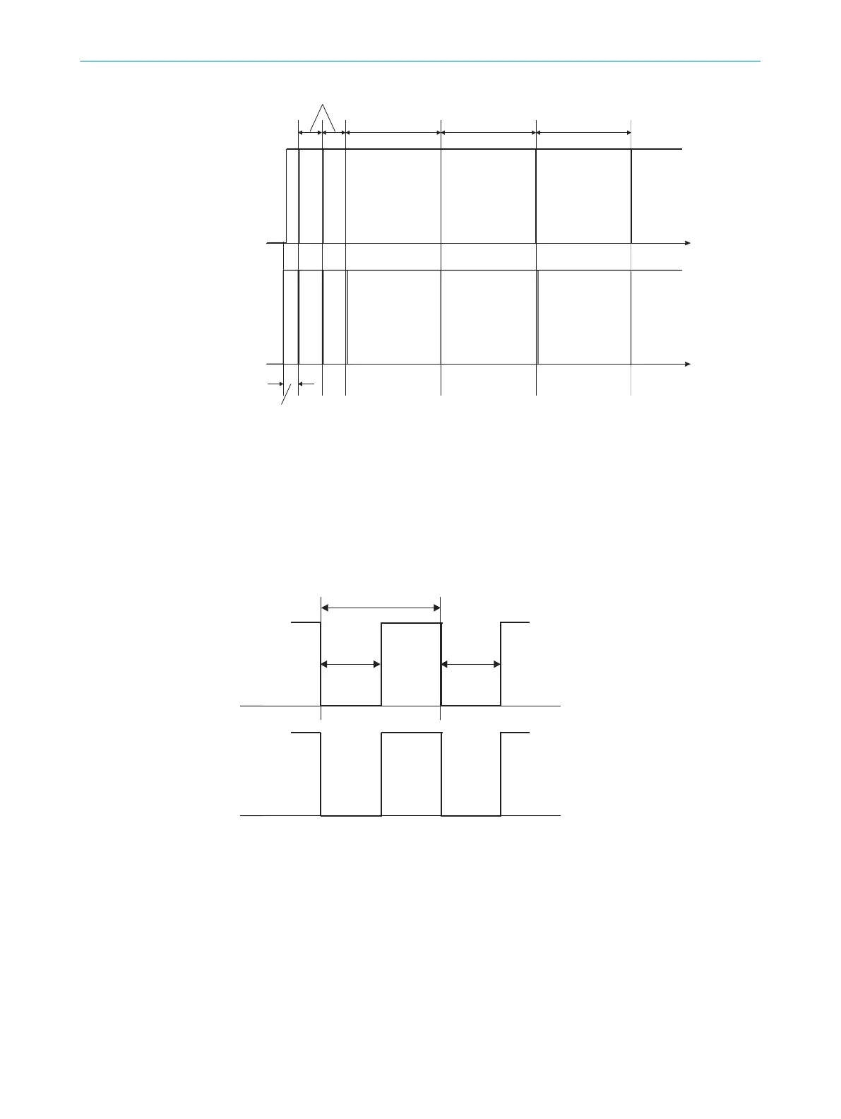
≈ 35 ms
1 2 31 2 3
OSSD2
O
SSD1
40 ms
120 ms 120 ms 120 ms
t
t
Figure 74: Diagram of the test pulse at the OSSDs
Appr
ox. 35 ms after the OSSDs are switched on, the device performs the first voltage
test 1. Then, after a half basic response time (40 ms), it performs a second voltage
test 1.
After a further half basic response time of the device there is a shut-down test 2,
120 ms later a further voltage test 3. Then the device performs a shut-down test and a
voltage test alternately at an interval of 120 ms. Pulse duration for the individual tests,
see figure 75, page 117, see figure 76, page 118, see figure 77, page 118.
≈ 650 μs
< 300 μs < 300 μs
OSSD2
OSSD1
Figure 75: Voltage test after switching on the OSSDs
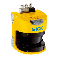
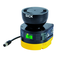
TECHNICAL DATA 12
8014170/ZA23/2019-11-14 | SICK O P E R A T I N G I N S T R U C T I O N S | S300 Mini
117
Subject to change without notice