Function diagram
87654321
fp_mc_180_e.vsd
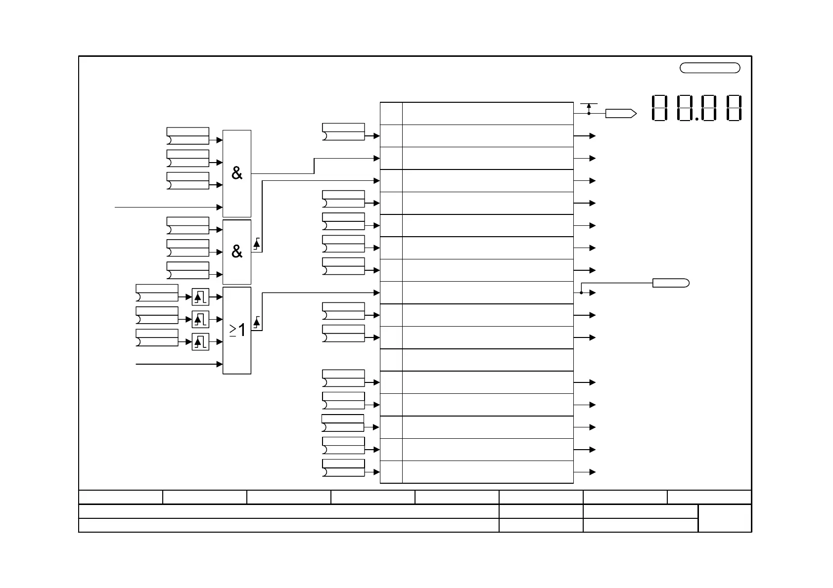
Control word 1
MASTERDRIVES MC
10.02.03
-180 -
V2.5
"Safe STOP" check-back 3)
from PMU [50.7]
Bit 1
Bit 2
Bit 3
Bit 4
Bit 5
Bit 6
Bit 7
Bit 8
Bit 9
Bit 10
Bit 11
Bit 12
Bit 13
Bit 14
Bit 15
0=OFF1,Shutdown via ramp-function generator, followed
by pulse disable
1=ON, operating conditions (edge-controlled)
Meaning
0=OFF2,Pulse disable, motor coasts down
1=Operating condition
0=OFF3, Quick stop
1=Operating condition
1=Inverter enable, pulse enable
0=Pulse disable
1=Ramp-function-generator enable
0=Set ramp-function generator to 0
1=Start ramp-function generator
0=Stop ramp-function generator
1=Setpoint enable
0=Setpoint disable
0 => 1 Edge fault acknowledgement
1=Inching bit 0
1=Inching bit 1
1=Control requested
0=No control requested
1=Clockwise phase sequence enable
0=Clockwise phase sequence disable
1=Counter-clockwise phase sequence enable
0=Counter-clockwise phase sequence disable
1=Raise mot. potentiometer
0=External fault 1 (F035),
1=No external fault
1=Lower mot. potentiometer
to sequence control 1)
to sequence control 1)
to sequence control 1)
to sequence control 1)
to sequence control 1)
to setpoint processing (part 2) [320.2]
to setpoint processing (part 1) [310.7]
to sequence control 1)
to sequence control 1)
to sequence control 1)
to setpoint processing (part 1) [310.7]
to mot. potentiometer [300.2]
to mot. potentiometer [300.2]
to sequence control 1)
to fault processing
Note: This bit must be set in the first PcD word of the
telegram received from the serial interfaces so that the
converter will accept the process data as valid (compare
USS, Profibus etc.; does not apply to SIMOLINK)
Bit No.
Bit 0
to setpoint processing (part 2) [320.2]
The sequence control system is the
internal control system (software) for
implementing the drive status (r001).
Pre-assignment of the BICO parameters:
1. Binector valid for BICO data set 1
2. Binector valid for BICO data set 2
Pulse generator
15 14
76
13 12
54
11 10
32
98
10
Display of r550 on the PMU
The signal remains high on acknowledgement at least
for T10 (= 204.8 ms with 5 kHz pulse frequency).
2)
1)
For Compact PLUS devices from function
diagram 91.4 or 92.4: Only evaluated in the
"Ready for switching on" state (r001 = 9) with
compact and chassis devices.
3)
B
P555.B (1/20)
Src1 OFF2(coast)
B
P556.B (1/1)
Src2 OFF2(coast)
B
P557.B (1/1)
Src3 OFF2(coast)
B
P558.B (1/1)
Src1 OFF3(QStop)
B
P559.B (1/1)
Src2 OFF3(QStop)
B
P560.B (1/1)
Src3 OFF3(QStop)
B
P565.B(2107)
Src1 Fault Reset
B
P566.B (0/0)
Src2 Fault Reset
B
P567.B (0/18)
Src3 Fault Reset
B
P554.B (0/0)
Src ON/OFF1
B
P561.B (1/1)
Src InvRelease
B
P562.B (1/1)
Src RampGen Rel
B
P563.B (1/1)
Src RampGen Stop
B
P564.B (1/1)
Src Setp Release
B
P568.B (0/0)
Src Jog Bit0
B
P569.B (0/0)
Src Jog Bit1
B
P571.B (1/1)
Src FWD Speed
B
P572.B (1/1)
Src REV speed
B
P574.B (0/0)
Src MOP Down
B
P575.B (1/1)
Src No ExtFault1
B
P573.B (0/0)
Src MOP UP
Control word 1
r550
K0030
Control word 1
n959.25 = 4
B0094 Fault acknowl. 2)
 Loading...