B.4 Parameter Defaults Determined by Control Mode (A1-02)
YASKAWA ELECTRIC SIEP C710616 30B YASKAWA AC Drive T1000A Technical Manual 423
Parameter List
B
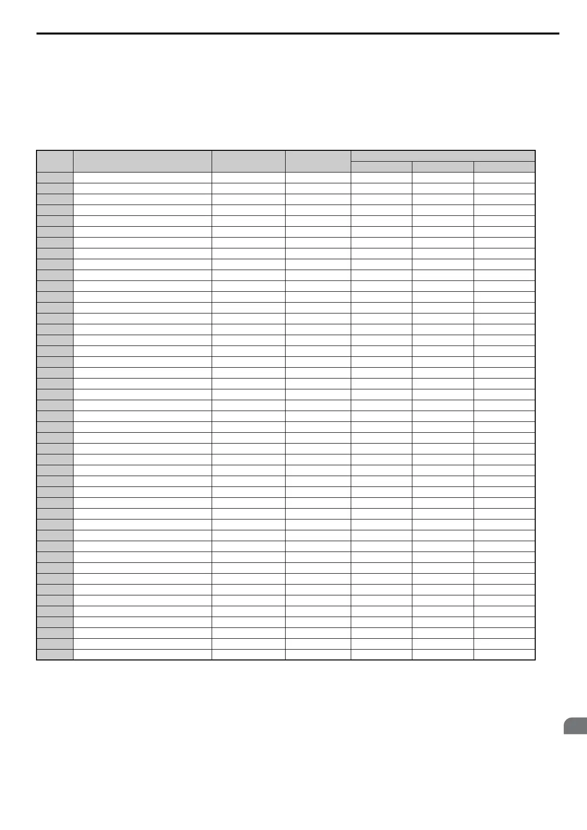
Table B.3 A1-02 (Motor 1 Control Mode) Dependent Parameters and Default Values
<5> Default setting value varies by the drive model (o2-04).
y CIMR-T2A0004 to 2A0021, CIMR-T4A0002 to 4A0011: 15.0V
y CIMR-T2A0030 to 2A0211, CIMR-T4A0018 to 4A0103: 14.0V
y CIMR-T2A0250 to 2A0415, CIMR-T4A0139 to 4A0362: 12.0V
<6> Default setting value varies by the drive model (o2-04).
y CIMR-T2A0004 to 2A0021, CIMR-T4A0002 to 4A0011: 9.0V
y CIMR-T2A0030 to 2A0211, CIMR-T4A0018 to 4A0103: 7.0V
y CIMR-T2A0250 to 2A0415, CIMR-T4A0139 to 4A0362: 6.0V
No. Name Setting Range Resolution
Control Modes (A1-02)
OLV/PM (5) AOLV/PM (6) CLV/PM (7)
b2-01 DC Injection Braking Start Frequency 0.0 to 10.0 0.1 Hz 0.5 1.0% <1> 0.5% <1>
b2-04
<1> This default setting is calculated as a percentage of the maximum output frequency.
<2> In AOLV/PM and CLV/PM control modes, the setting units and range are expressed as a percent (0.0 to 100.0%) instead of in Hz.
<3> Default setting value is dependent on the motor code set to parameter E5-01.
<4> In AOLV/PM and CLV/PM control modes, the setting units and range are expressed as a percent (-100.0 to 100.0%) instead of in Hz.
<5> Values shown here are for 200 V class drives. Double the value when using a 400 V class drive.
DC Injection Braking Time at Stop 0.00 to 10.00 0.01 s 0.50 – 0.50
b2-13 Short Circuit Brake Time at Stop 0.00 to 25.50 0.01 s 0.50 0.00 –
b3-01 Speed Search Selection at Start 0 to 1 – 0 0 –
b3-02 Speed Search Deactivation Current 0 to 200 1% – – –
b3-14 Bi-Directional Speed Search Selection 0,1 – – – –
b5-15 PID Sleep Function Start Level 0.0 to 400.0 <2> 0.1 0.0 Hz 0.0% 0.0%
b6-01 Dwell Reference at Start 0.0 to 400.0 <2> 0.1 0.0 Hz 0.0% 0.0%
b6-03 Dwell Reference at Stop 0.0 to 400.0 <2> 0.1 0.0 Hz 0.0% 0.0%
b8-01 Energy Saving Control Selection 0 to 1 – – 1 1
b8-02 Energy Saving Gain 0.0 to 10.0 0.1 – – –
b8-03 Energy Saving Control Filter Time Constant 0.00 to 10.00 0.01 s – – –
C1-11 Accel/Decel Time Switching Frequency 0.0 to 400.0 <2> 0.1 0.0 Hz 0.0% 0.0%
C2-01 S-Curve Time at Acceleration Start 0.00 to 10.00 0.01 s 1.00 1.00 1.00
C3-01 Slip Compensation Gain 0.0 to 2.5 0.1 – – –
C3-02 Slip Compensation Primary Delay Time 0 to 10000 1 ms – – –
C4-01 Torque Compensation Gain 0.00 to 2.50 0.01 0.00 – –
C4-02 Torque Compensation Primary Delay Time 0 to 10000 1 ms 100 – –
C5-01 ASR Proportional Gain 1 0.00 to 300.00 0.01 – – –
C5-02 ASR Integral Time 1 0.000 to 10.000 0.001 s – – –
C5-03 ASR Proportional Gain 2 0.00 to 300.00 0.01 – – –
C5-04 ASR Integral Time 2 0.000 to 10.000 0.001 s – – –
C5-06 ASR Primary Delay Time Constant 0.000 to 0.500 0.001 s – – –
C5-07 ASR Gain Switching Frequency 0.0 to 400.0 <2> 0.1 – 0.0% 0.0%
C6-02 Carrier Frequency Selection 1 to F – 2 2 2
E1-04 Maximum Output Frequency 40.0 to 400.0 0.1 Hz <3> <3> <3>
E1-05 Maximum Voltage <5> 0.0 to 255.0 0.1 V <3> <3> <3>
E1-06 Base Frequency 0.0 to 400.0 0.1 Hz <3> <3> <3>
E1-07 Middle Output Frequency 0.0 to 400.0 0.1 Hz – – –
E1-08 Middle Output Frequency Voltage <5> 0.0 to 255.0 0.1 V – – –
E1-09 Minimum Output Frequency 0.0 to 400.0 0.1 Hz <3> <3> <3>
E1-10 Minimum Output Frequency Voltage <5> 0.0 to 255.0 0.1 V – – –
F1-05 PG 1 Rotation Selection 0 to 1 – – – 1
F1-09 Overspeed Detection Delay Time 0.0 to 2.0 0.1 s – 0.0 0.0
L1-01 Motor Overload Protection Selection 0 to 6 – 4 4 5
L4-01 Speed Agreement Detection Level 0.0 to 400.0 <2> 0.1 0.0 Hz 0.0% 0.0%
L4-02 Speed Agreement Detection Width 0.0 to 20.0 0.1 Hz 2.0 4.0% <1> 4.0% <1>
L4-03 Speed Agreement Detection Level (+/-) -400.0 to 400.0 <4> 0.1 0.0 Hz 0.0% 0.0%
L4-04 Speed Agreement Detection Width (+/-) 0.0 to 20.0 0.1 Hz 2.0 4.0% <1> 4.0% <1>
L8-38 Carrier Frequency Reduction Selection 0 to 2 – 0 – 0
L8-40 Carrier Frequency Reduction Off Delay Time 0.00 to 2.00 0.01 s 0.00 – 0.00
o1-03 Digital Operator Display Selection 0 to 3 – 0 1 1
o1-04 V/f Pattern Display Unit 0, 1 – – 1 1
S6-04 DC Bus Adjustment Gain 0.00 to 5.00 0.01 0.65 0.65 0.65
S6-07 Torque Limit Delay Time 0.000 to 1.000 0.001 s – 0.200 0.020

 Loading...