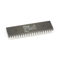
Z8 Microcontrollers
Power-Down Modes ZiLOG
8-2 UM001601-0803
8.3 STOP MODE OPERATION
The STOP mode provides the lowest possible device standby
current. This instruction turns off the on-chip oscillator and in
-
ternal system clock.
To enter the STOP mode, it is necessary to first flush the instruc-
tion pipeline to avoid suspending execution in mid-instruction.
To do this, the application program must execute a NOP instruc
-
tion (opcode=FFH) immediately before the STOP instruction
(opcode=6FH), that is,
The STOP mode is exited by any one of the following resets:
Power-On Reset activation, WDT time out (if available), or a
STOP-Mode Recovery source. Upon reset generation, the pro
-
cessor will always restart the application program at address
000CH.
POR/RESET activation is present on all Z8 devices and is imple-
mented as a reset pin and/or an on-chip power on reset circuit.
Some Z8 devices allow for the on-chip WDT to run in the STOP
mode. If so activated, the WDT timeout will generate a reset
some fixed time period after entering the STOP mode.
Note: STOP-Mode Recovery by the WDT will increase the
STOP mode standby current (I
CC2
). This is due to the WDT
clock and divider circuitry that is now enabled and running to
support this recovery mode. See the product data sheet for actual
I
CC2
values.
All Z8 devices provide some form of dedicated STOP-Mode Re-
covery (SMR) circuitry. Two SMR methods are implemented —
a single fixed input pin or a flexible, programmable set of inputs.
The selected Z8 device product specification should be reviewed
to determine the SMR options available for use.
Note: For devices that support SPI, the slave mode compare
feature also serves as a SMR source.
In the simple case, a low level applied to input pin P27 will trig-
ger a SMR. To use this mode, pin P27 (I/O Port 2, bit 7) must be
configured as an input before the STOP mode is entered. The
low level on P27 must meet a minimum pulse width T
WSM
. (See
the product data sheet) to trigger the device reset mode). Some
Z8 devices provide multiple SMR input sources. The desired
SMR source is selected via the SMR Register.
Note: Use of specialized SMR modes (P2.7 input or SMR
register based) or the WDT timeout (only when in the STOP
mode) provide a unique reset operation. Some control registers
are initialized differently for a SMR/WDT triggered POR than a
standard reset operation. See the product specification (register
file map) for exact details.
To determine the actual STOP mode current (I
CC2
) value for the
optional SMR modes available, see the selected Z8 device’s
product data sheet.
Note: The STOP mode current (I
CC2
) will be minimized when:
•V
CC
is at the low end of the devices operating range.
• WDT is off in the STOP mode.
• Output current sourcing is minimized.
• All inputs (digital and analog) are at the low or high rail
voltages.
FF NOP ;clear the instruction pipeline
6F STOP ;enter STOP mode

 Loading...