Z8 Microcontrollers
Serial I/O ZiLOG
9-6 UM001601-0803
9.4 TRANSMITTER OPERATION
The transmitter consists of a transmitter buffer (SIO Register
[F0H]), a parity generator, and associated control logic. The
transmitter block diagram is shown as part of Figure 9-1.
After a hardware reset or after a character has been transmitted,
the transmitter is forced to a marking state (output always High)
until a character is loaded into the transmitter buffer, SIO Regis
-
ter (F0H). The transmitter is loaded by specifying the SIO Reg-
ister as the destination register of any instruction.
T0’s output drives a divide-by-16 counter that in turn generates
a shift clock every 16 counts. This counter is reset when the
transmitter buffer is written by an instruction. This reset syn
-
chronizes the shift clock to the software. The transmitter then
outputs one bit per shift clock, through Port 3 bit 7, until a start
bit, the character written to the buffer, and two stop bits have
been transmitted. After the second stop bit has been transmitted,
the output is again forced to a marking state. Interrupt request
IRQ4 is generated at this time to notify the processor that the
transmitter is ready to accept another character.
9.4.1 Overwrites
The user is not protected from overwriting the transmitter, so it
is up to the software to respond to IRQ4 appropriately. If polling
is used, the IRQ4 bit in the Interrupt Request Register must be
reset.
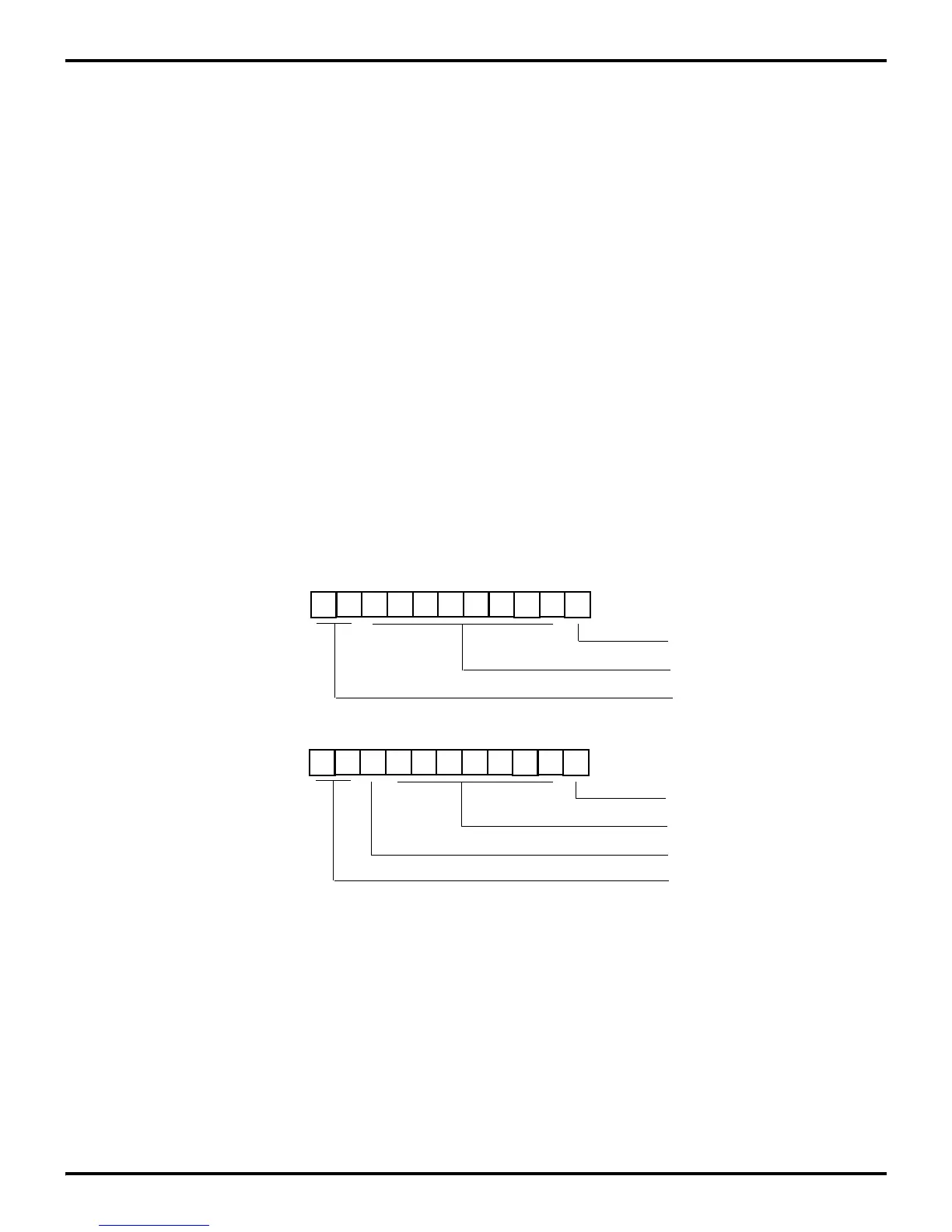
9.4.2 Parity
The data format supported by the transmitter has a start bit, eight
data bits, and at least two stop bits. If parity is on, bit 7 of the data
transmitted will be replaced by an odd parity bit. Figure 9-9
shows the transmitter data formats.
Parity is enabled by setting Port 3 Mode Register bit 7 to 1. If
even parity is required, the parity mode should be disabled (P3M
bit 7 reset to 0), and software must modify the data to include
even parity.
Since the transmitter can be overwritten, the user is able to gen-
erate a break signal. This is done by writing null characters to the
transmitter buffer (SIO Register [F0H]) at a rate that does not al
-
low the stop bits to be output. Each time the SIO Register is load-
ed, the divide-by-16 counter is resynchronized and a new start
bit is output followed by data.
Figure 9-9. Transmitter Data Formats
SP SP D7 D6 D5 D4 D3 D2 D1 D0 ST
Eight Data Bits
Start Bit
Start Bit
Seven Data Bits
Two Stop Bit
SP SP P D6 D5 D4 D3 D2 D1 D0 ST
Odd Parity
Two Stop Bit
Transmitted Data
(No Parity)
Transmitted Data
(With Parity)

 Loading...
