Z8 Microcontrollers
ZiLOG I/O Ports
UM001601-0803 5-29
For Z8s having the PCON register feature, the following bits
control the Low EMI options:
• Low EMI Port 0 (D3). Port 0 can be configured as a Low
EMI Port by resetting this bit (D3=0) or configured as a
Standard Port by setting this bit (D3=1). The default value is 1.
• Low EMI Port 1 (D4). Port 1 can be configured as a Low
EMI Port by resetting this bit (D4=0) or configured as a
Standard Port by setting this bit (D4=1). The default value is 1.
• Low EMI Port 2 (D5). Port 2 can be configured as a Low
EMI Port by resetting this bit (D5=0) or configured as a
Standard Port by setting this bit (D5=1). The default value is 1.
• Low EMI Port 3 (D6). Port 3 can be configured as a Low
EMI Port by resetting this bit (D6=0) or configured as a
Standard Port by setting this bit (D6=1). The default value is 1.
• Low EMI OSC (D7). This bit of the PCON Register controls
the Low EMI oscillator. A 1 in this location configures the
oscillator with standard drive, while a 0 configures the
oscillator with low noise drive. The Low-EMI mode will
reduce the drive of the oscillator (OSC). The default value is
1. XTAL/2 mode is not effected by this bit.
Note: The maximum external clock frequency is 4 MHz when
running in the Low EMI oscillator mode.
Please refer to the selected device product specification for
availability of the Low EMI feature and programming options.
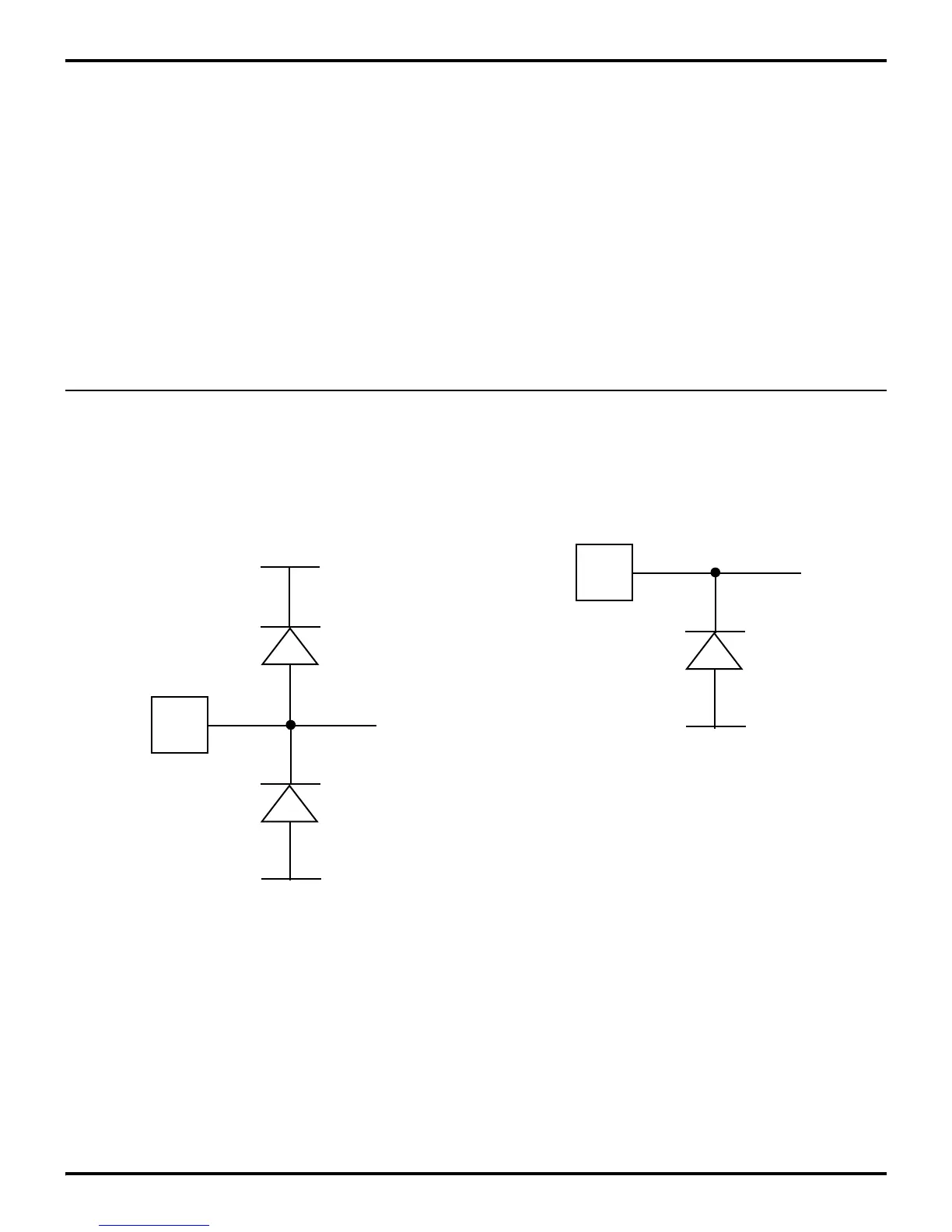
5.11 INPUT PROTECTION
All CMOS ROM Z8s have I/O pins with diode input protection.
There is a diode from the I/O pad to V
CC
and to V
SS
. See Figure
5-36.
On CMOS OTP EPROM Z8s, the Port 3 inputs P31, P32, P33
and the XTAL 1 pin have only the input protection diode from
pad to V
SS
. See Figure 5-37.
The high-side input protection diodes were removed on these
pins to allow the application of +12.5V during the various OTP
programming modes.
For better noise immunity in applications that are exposed to
system EMI, a clamping diode to V
CC
from these pins may be re-
quired to prevent entering the OTP programming mode or to pre-
vent high voltage from damaging these pins.
Figure 5-36. Diode Input Protection
PIN
V
CC
V
SS
Figure 5-37. OTP Diode Input Protection
PIN
V
SS