Z8 Microcontrollers
Serial I/O ZiLOG
9-8 UM001601-0803
9.6 SERIAL PERIPHERAL INTERFACE (SPI)
Select Z8 microcontrollers incorporate a serial peripheral inter-
face (SPI) for communication with other microcontrollers and
peripherals. The SPI includes features such as Stop-Mode Re
-
covery, Master/Slave selection, and Compare mode. Table 9-3
contains the pin configuration for the SPI feature when it is en
-
abled. The SPI consists of four registers: SPI Control Register
(SCON), SPI Compare Register (SCOMP), SPI Receive/Buffer
Register (RxBUF), and SPI Shift Register. SCON is located in
bank (C) of the Expanded Register File at address 02.
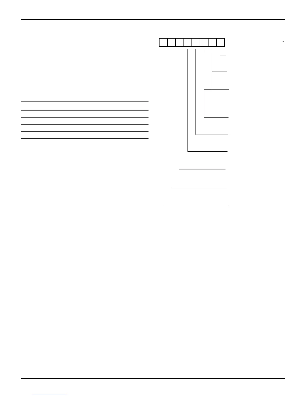
The SPI Control Register (SCON) (Figure 9-12), is a read/write
register that controls Master/Slave selection, interrupts, clock
source and phase selection, and error flag. Bit 0 enables/disables
the SPI with the default being SPI disabled. A 1 in this location
will enable the SPI, and a 0 will disable the SPI. Bits 1 and 2 of
the SCON register in Master Mode select the clock rate. The user
may choose whether internal clock is divide-by-2, 4, 8, or 16. In
Slave Mode, Bit 1 of this register flags the user if an overrun of
the RxBUF Register has occurred. The RxCharOverrun flag is
only reset by writing a 0 to this bit. In slave mode, bit 2 of the
Control Register disables the data-out I/O function. If a 1 is writ
-
ten to this bit, the data-out pin is released to its original port con-
figuration. If a 0 is written to this bit, the SPI shifts out one bit
for each bit received. Bit 3 of the SCON Register enables the
compare feature of the SPI, with the default being disabled.
When the compare feature is enabled, a comparison of the value
in the SCOMP Register is made with the value in the RxBUF
Register. Bit 4 signals that a receive character is available in the
RxBUF Register.
If the associated IRQ3 is enabled, an interrupt is generated. Bit
5 controls the clock phase of the SPI. A 1 in bit 5 allows for re
-
ceiving data on the clock’s falling edge and transmitting data on
the clock’s rising edge. A 0 allows receiving data on the clock’s
rising edge and transmitting on the clock’s falling edge. The SPI
clock source is defined in bit 6. A 1 uses Timer0 output for the
SPI clock, and a 0 uses TCLK for clocking the SPI. Finally, bit
7 determines whether the SPI is used as a Master or a Slave. A 1
puts the SPI into Master mode and a 0 puts the SPI into Slave
mode.
Table 9-3. SPI Pin Configuration
Name Function Pin Location
DI Data-In P20
DO Data-Out P27
SS Slave Select P35
SK SPI Clock P34
Figure 9-12. SPI Control Register (SCON)
D7 D6 D5 D4 D3 D2 D1 D0
SCON (C) 02
CLK Divide (M)
00 TCLK/2
01 TCLK/4
10 TCLK/8
11 TCLK/16
DO SPI Port Enable (S)
0 SPI DO Port Enable
1 Do Port to I/O
0 Disable *
1 Enable
SPI Enable
0 Enable
1 Disable *
Compare Enable
0 Trans/Fall
1 Trans/Rise
Clock Phase
0 Reset
RxCharOverrun (S)
0 Reset
1 Char. Avail
RxCharAvail
1 Overrun
(M) Used with Bit D7 equal to 1
* Default setting after Reset
0 TCLK
1 Timer 0 Output
CLK Source
0 Slave
1 Master
Master Slave
(S) Used with Bit D7 equal to 0

 Loading...
