Z8 Microcontrollers
Serial I/O ZiLOG
9-4 UM001601-0803
The bit rate generator is started by setting the Timer Mode Reg-
ister (TMR) (F1H) bit 1 and bit 0 both to 1 (Figure 9-5). This
transfers the contents of the Prescaler 0 Register and
Counter/Timer0 Register to their corresponding down counters.
In addition, counting is enabled so that UART operations begin.
9.3 UART RECEIVER OPERATION
The receiver consists of a receiver buffer (SIO Register [F0H]),
a serial-in, parallel-out shift register, parity checking, and data
synchronizing logic. The receiver block diagram is shown as
part of Figure 9-1.
9.3.1 Receiver Shift Register
After a hardware reset or after a character has been received, the
Receiver Shift Register is initialized to all 1s and the shift clock
is stopped. Serial data, input through Port 3 bit 0, is synchronized
to the internal clock by two D-type flip-flops before being input
to the Shift Register and the start bit detection circuitry.
The start bit detection circuitry monitors the incoming data
stream, looking for a start bit (a High-to-Low input transition).
When a start bit is detected, the shift clock logic is enabled. The
T0 input is divided-by-16 and, when the count equals eight, the
divider outputs a shift clock. This clock shifts the start bit into
the Receiver Shift Register at the center of the bit time. Before
the shift actually occurs, the input is rechecked to ensure that the
start bit is valid. If the detected start bit is false, the receiver is
reset and the process of looking for a start bit is repeated. If the
start bit is valid, the data is shifted into the Shift Register every
sixteen counts until a full character is assembled (Figure 9-6).
Figure 9-5. Timer Mode Register (TMR) Bit Rate Generation
D7 D6 D5 D4 D3 D2 D1 D0
(Read/Write)
0 = No Function
1 = Load T
0
Timer Mode Register (TMR)
Register F1H
0 = Disable T
0
Count
1 = Enable T
0
Count
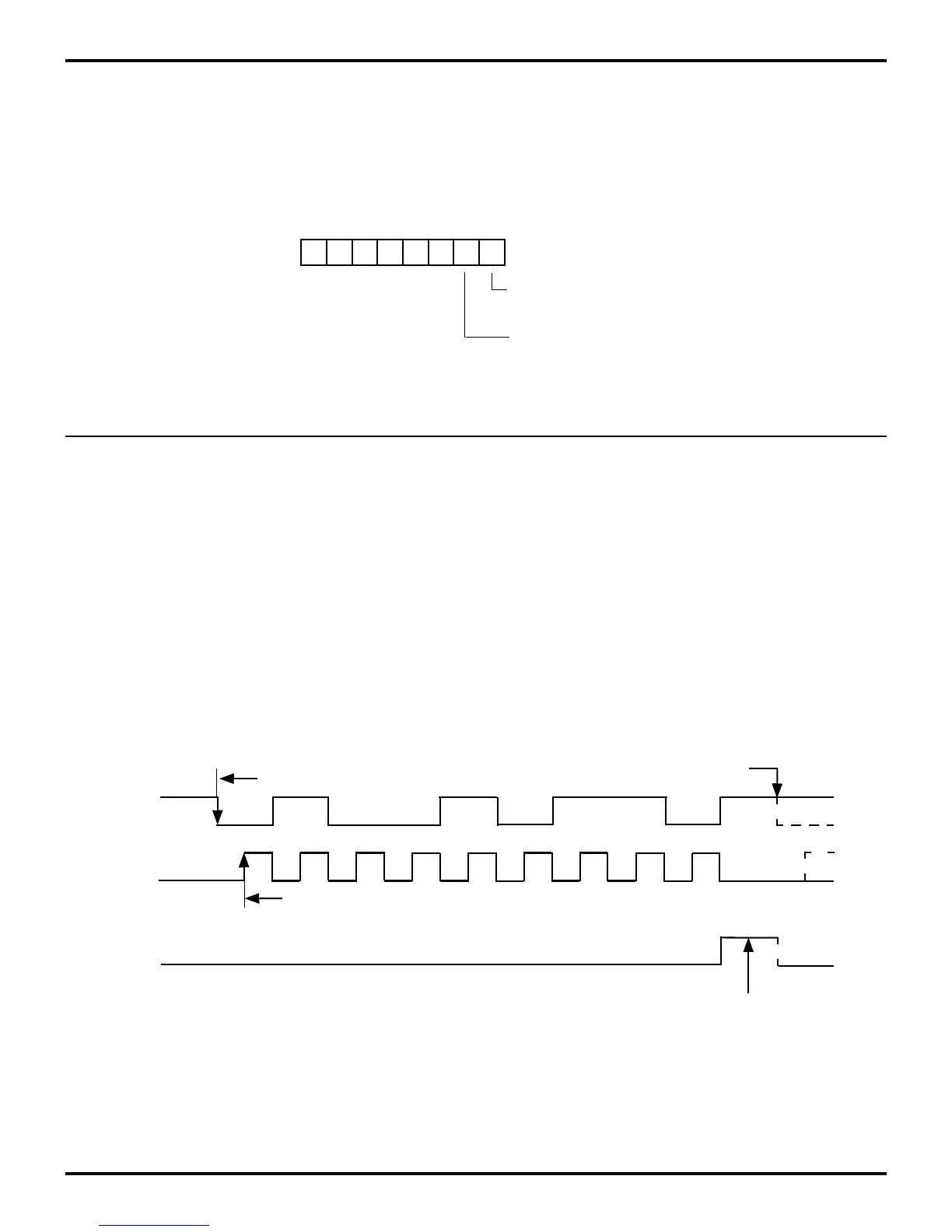
Figure 9-6. Receiver Timing
Shift register Contents
(R)
Shift
RCVR
Start Bit Transition Detected
Eight T0 Counts Later Shifting Starts
Stop Bit
One or More
Transferred to Receive Buffer
and IRQ3 is Generated
RCVR
Data
Clock
IRQ3