Z8 Microcontrollers
ZiLOG Power-Down Modes
UM001601-0803 8-3
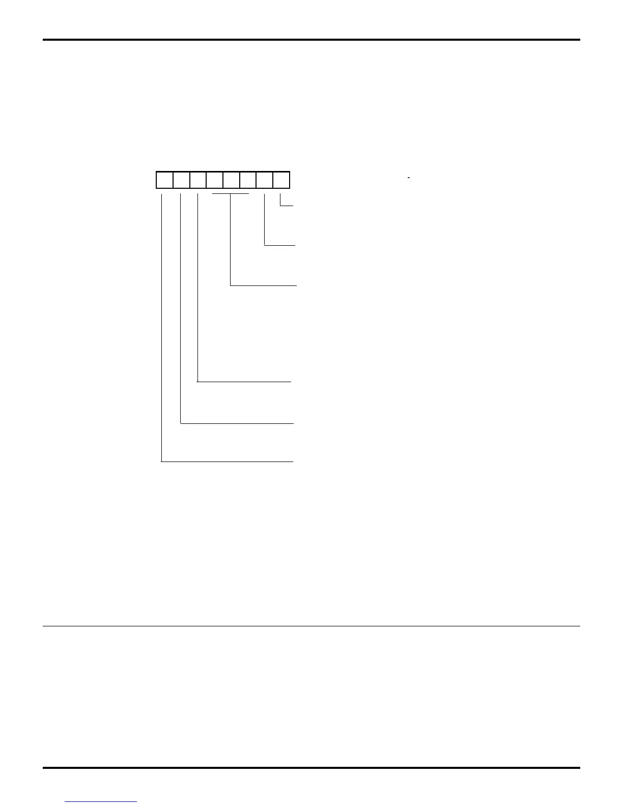
8.4 STOP-MODE RECOVERY REGISTER
This register selects the clock divide value and determines the
mode of STOP-Mode Recovery (Figure 8-1). All bits are Write-
Only, except bit 7, that is Read-Only. Bit 7 is a flag bit that is
hardware set on the condition of STOP recovery and reset by a
power-on cycle. Bit 6 controls whether a low level or a high level
is required from the recovery source. Bit 5 controls the reset de
-
lay after recovery. Bits 2, 3, and 4, of the SMR register, specify
the source of the STOP-Mode Recovery signal. Bits 0 and 1 con
-
trol internal clock divider circuitry. The SMR is located in Bank
F of the Expanded Register File at address 0BH.
Note: The SMR register is available in select Z8 MCU products. Refer to the device product specification to determine SMR options
available.
SCLK/TCLK Divide-by-16 Select (DO). This bit of the SMR
controls a divide-by-16 prescaler of SCLK/TCLK. The purpose
of this control is to selectively reduce device power consumption
during normal processor execution (SCLK control) and/or
HALT mode (where TCLK sources counter/timers and interrupt
logic).
External Clock Divide-by-Two (D1). This bit can eliminate the
oscillator divide-by-two circuitry. When this bit is 0, the System
Clock (SCLK) and Timer Clock (TCLK) are equal to the exter
-
nal clock frequency divided by two. The SCLK/TCLK is equal
to the external clock frequency when this bit is set (D1=1). Using
this bit together with D7 of PCON helps further lower EMI (D7
(PCON) =0, D1 (SMR) =1). The default setting is zero.
Figure 8-1. STOP-Mode Recovery Register
(Write-Only Except Bit D7, Which Is Read-Only)
D7 D6 D5 D4 D3 D2 D1 D0
SMR (FH) 0B
STOP-Mode Recovery Source
000 POR Only and/or External Reset
001 P30
010 P31
011 P32
100 P33
101 P27
110 P2 NOR 0-3
111 P2 NOR 0-7
0 OFF **
1 ON
SCLK/TCLK Divide-by-16
0 OFF
1 ON*
Stop Delay
0 POR*
1 Stop Recovery
Stop Flag (Read Only)
0 SCLK/TCLK = XTAL/2*
External Clock Divide by 2
0 Low*
1 High
Stop Recovery Level
1 SCLK/TCLK = XTAL
* Default setting after RESET.
** Default setting after RESET and STOP-Mode Recovery.

 Loading...
