Z8 Microcontrollers
Power-Down Modes ZiLOG
8-4 UM001601-0803
8.4 STOP-MODE RECOVERY REGISTER (Continued)
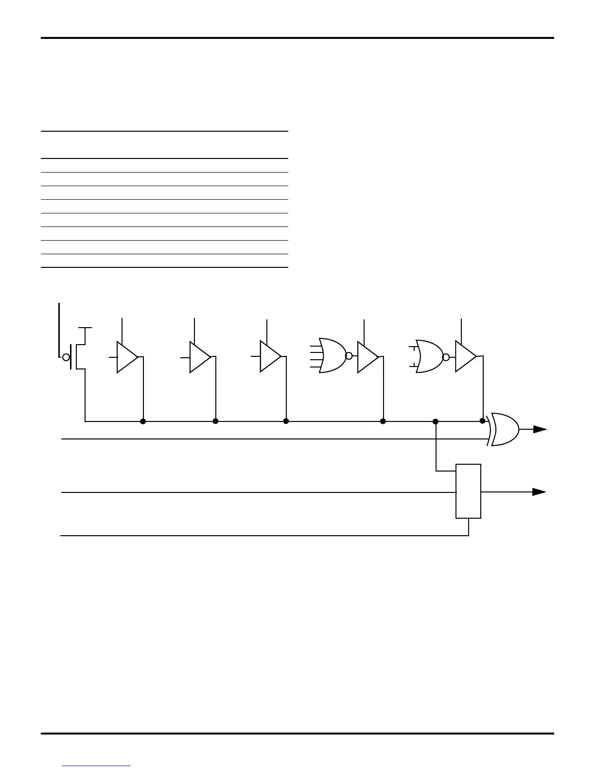
STOP-Mode Recovery Source (D2, D3, and D4). These three
bits of the SMR specify the wake-up source of the STOP recov
-
ery and (Table 8-1 and Figures 8-2).
STOP-Mode Recovery Delay Select (D5). This bit, if High, en-
ables the T
POR
/RESET delay after Stop-Mode Recovery. The
default configuration of this bit is 1. If the “fast” wake up is se
-
lected, the Stop-Mode Recovery source is kept active for at least
5 TpC.
STOP-Mode Recovery Edge Select (D6). A 1 in this bit posi-
tion indicates that a high level on any one of the recovery sources
wakes the Z8 from STOP mode. A 0 indicates low-level recov
-
ery. The default is 0 on POR (Figure 8-2).
Cold or Warm Start (D7). This bit is set by the device upon en-
tering STOP mode. A 0 in this bit (cold) indicates that the device
reset by POR/WDT RESET. A 1 in this bit (warm) indicates that
the device awakens by a SMR source.
Note: If P31, P32, or P33 are to be used for a SMR source, the digital mode of operation must be selected prior to entering the STOP
Mode.
Table 8-1. STOP-Mode Recovery Source
SMR: 432 Operation
D4 D3 D2 Description of Action
0 0 0 POR and/or external reset recovery
0 0 1 P30 transition
0 1 0 P31 transition (not in Analog Mode)
0 1 1 P32 transition (not in Analog Mode)
1 0 0 P33 transition (not in Analog Mode)
1 0 1 P27 transition
1 1 0 Logical NOR of P20 through P23
1 1 1 Logical NOR of P20 through P27
Figure 8-2. STOP-Mode Recovery Source
SMR D4 D3 D2
0 0 0
SMR D4 D3 D2
0 0 1
0 1 0
0 1 1
SMR D4 D3 D2
1 0 0
SMR D4 D3 D2
1 0 1
SMR D4 D3 D2
1 1 0
SMR D4 D3 D2
1 1 0
V
DD
P20
P23
P20
P27
P30
P33
P27
P31
P32
MUX
To POR
RESET
To P33 Data
Latch and IRQ
1
Stop Mode Recovery Edge
Select (SMR)
P33 From Pads
Digital/Analog Mode
Select (P3M)

 Loading...
