Z8 Microcontrollers
Address Space ZiLOG
2-4 UM001601-0803
2.2 Z8 MCU STANDARD REGISTER FILE (Continued)
Note: The full register file is shown. Please refer to the selected device product specification for actual file size.
2.2.4 Error Conditions
Registers in the Z8 Standard Register File must be correctly used
because certain conditions produce inconsistent results and
should be avoided.
• Registers F3H and F5H-F9H are write-only registers. If an
attempt is made to read these registers, FFH is returned.
Reading any write-only register will return FFH.
• When register FDH (Register Pointer) is read, the least
significant four bits (lower nibble) will indicate the current
Expanded Register File Bank. (Example: 0000 indicates the
Standard Register File, while 1010 indicates Expanded
Register File Bank A.)
• When Ports 0 and 1 are defined as address outputs, registers
00H and 01H will return 1s in each address bit location when
read.
• Writing to bits that are defined as timer output, serial output,
or handshake output will have no effect.
• The Z8 instruction DJNZ uses any general-purpose working
register as a counter.
• Logical instructions such as OR and AND require that the
current contents of the operand be read. They therefore will
not function properly on write-only registers.
• The WDTMR register must be written within the first 60
internal system clocks (SCLK) of operation after a reset.
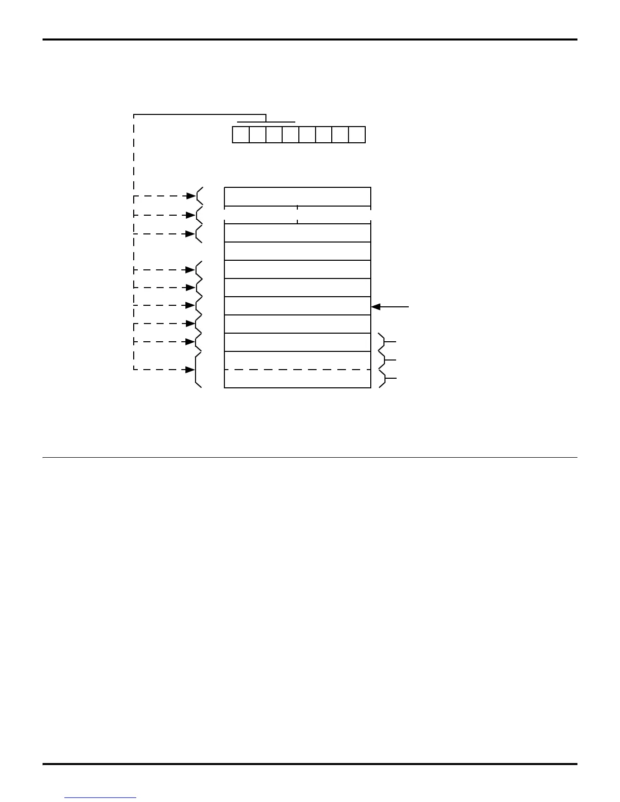
Figure 2-4. Register Pointer
FF
F0
R7 R6 R5 R4 R3 R2 R1 R0
Specified Working Register Group
R253
I/O Ports
Working Register Group 1
Working Register Group 0
Working Register Group F
EF
80
7F
70
6F
60
5F
50
4F
40
3F
30
2F
20
1F
10
0F
00
The lower nibble
of the register
file address
(provided by the
instruction) points
to the specified
register.
The upper nibble of the register file address,
provided by the register pointer, specifies
the active working-register group.
(Register Pointer)
R15 to R0
R15 to R4
R3 to R0

 Loading...
