Z8 Microcontrollers
External Interface ZiLOG
10-6 UM001601-0803
10.6 BUS OPERATION (Continued)
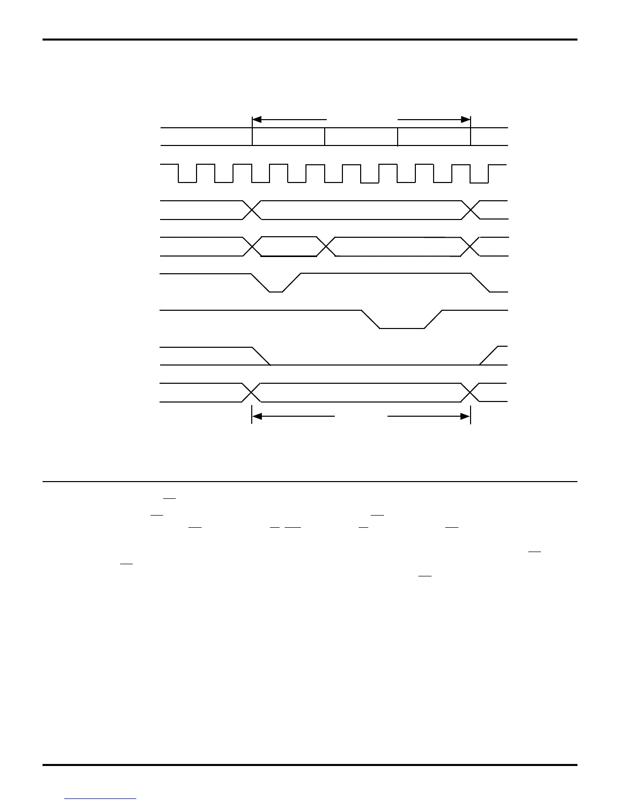
10.6.1 Address Strobe (AS)
All transactions start with AS driven Low and then raised High
by the Z8 MCU. The rising edge of
AS indicates that R/W, DM
(if used), and the address outputs are valid. The address outputs
(AD7-AD0), remain valid only during MnT1 and typically need
to be latched using
AS. Address outputs (A15-A8) remain stable
throughout the machine cycle, regardless of the addressing
mode.
10.6.2 Data Strobe (/DS)
The Z8 uses DS to time the actual data transfer. For Write oper-
ations (R/W = Low), a Low on DS indicates that valid data is on
the AD7-AD0 lines. For Read operations (R/W = High), the bus
is placed in a high-impedance state before driving
DS Low, so
the addressed device can put its data on the bus. The Z8 samples
this data prior to raising
DS High.
Figure 10-6. External Memory Write Cycle
Machine Cycle
T1
T2
T3
Clock
A15-A8
AD7-AD0
/AS
/DS
R/W
/DM
Write Cycle
A8-A15
A7-A0
D7-D0 OUT

 Loading...
