EasyManua.ls Logo

ZiLOG Z8 User Manual

ZiLOG Z8
220 pages
To Next Page IconTo Next Page
To Previous Page IconTo Previous Page
Page #22 background imageLoading...
Page #22 background image
Z8 Microcontrollers
Address Space ZiLOG
2-2 UM001601-0803
2.2 Z8 MCU STANDARD REGISTER FILE (Continued)
Registers can be accessed as either 8-bit or 16-bit registers using
Direct, Indirect, or Indexed Addressing. All 236 general-purpose
registers can be referenced or modified by any instruction that
accesses an 8-bit register, without the need for special
instructions. Registers accessed as 16 bits are treated as even-
odd register pairs (there are 118 valid pairs). In this case, the
data’s Most Significant Byte (MSB) is stored in the even
numbered register, while the Least Significant Byte (LSB) goes
into the next higher odd numbered register (Figure 2-1).
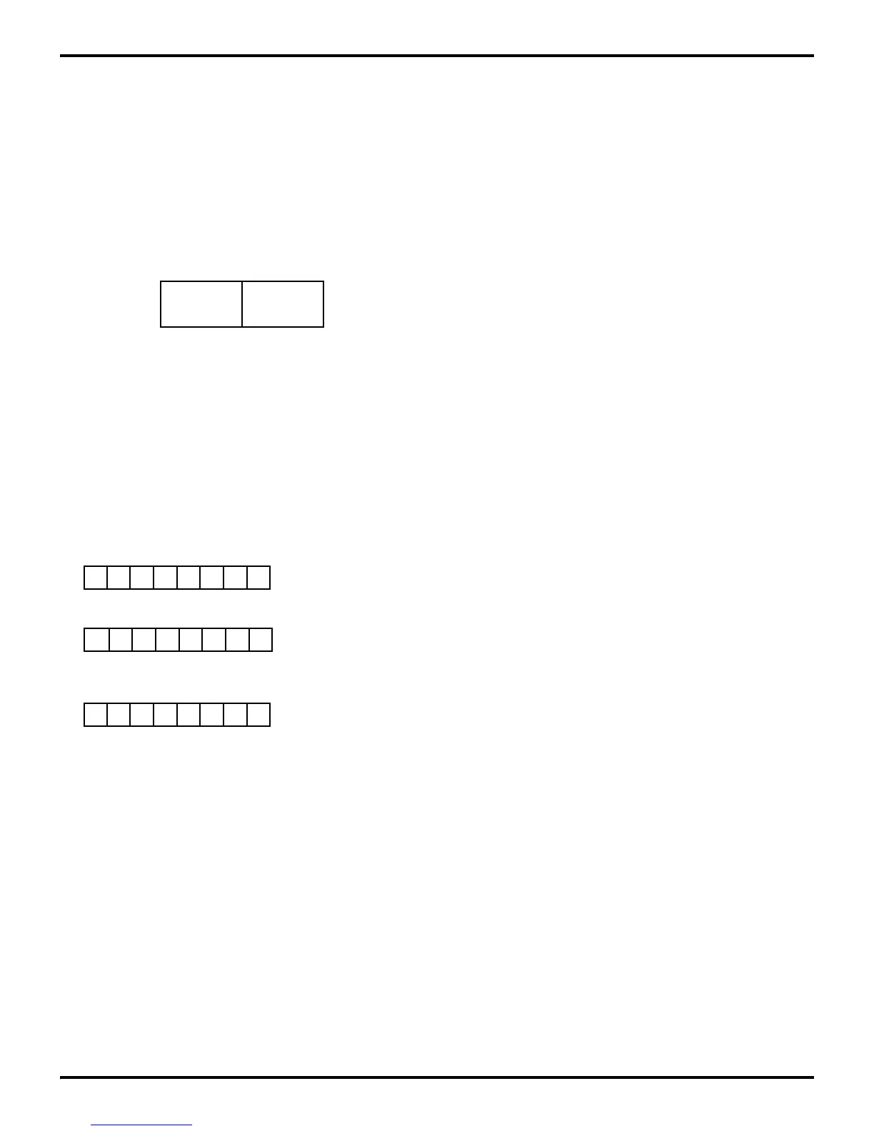
By using a logical instruction and a mask, individual bits within
registers can be accessed for bit set, bit clear, bit complement, or
bit test operations. For example, the instruction AND R15,
MASK performs a bit clear operation. Figure 2-2 shows this ex
-
ample.
When instructions are executed, registers are read when defined
as sources and written when defined as destinations. All Gener
-
al-Purpose Registers function as accumulators, address pointers,
index registers, stack areas, or scratch pad memory.
2.2.1 General-Purpose Registers
General-Purpose Registers (GPR) are undefined after the device
is powered up. The registers keep their last value after any reset,
as long as the reset occurs in the V
CC
voltage-specified operating
range. It will not keep its last state from a V
LV
reset if V
CC
drops
below 1.8v.
Note: Registers in Bank E0-EF may only be accessed through
the working register and indirect addressing modes. Direct
access cannot be used because the 4-bit working register address
mode already uses the format [E | dst], where dst represents the
working register number from 0H to FH.
2.2.2 RAM Protect
The upper portion of the register file address space 80H to EFH
(excluding the control registers) may be protected from reading
and writing. The RAM Protect bit option is mask-programmable
and is selected by the customer when the ROM code is submit
-
ted. After the mask option is selected, the user activates this fea-
ture from the internal ROM code to turn off/on the RAM Protect
by loading either a 0 or 1 into the IMR register, bit D6. A 1 in D6
enables RAM Protect. Only devices that use registers 80H to
EFH offer this feature.
2.2.3 Working Register Groups
Z8 instructions can access 8-bit registers and register pairs (16-
bit words) using either 4-bit or 8-bit address fields. 8-bit address
fields refer to the actual address of the register. For example,
Register 58H is accessed by calling upon its 8-bit binary equiv
-
alent, 01011000 (58H).
With 4-bit addressing, the register file is logically divided into
16 Working Register Groups of 16 registers each, as shown in
Table 2-2. These 16 registers are known as Working Registers.
A Register Pointer (one of the control registers, FDH) contains
the base address of the active Working Register Group. The high
nibble of the Register Pointer determines the current Working
Register Group.
When accessing one of the Working Registers, the 4-bit address
of the Working Register is combined within the upper four bits
(high nibble) of the Register Pointer, thus forming the 8-bit ac
-
tual address. Figure 2-3 illustrates this operation. Since working
registers are typically specified by short format instructions,
there are fewer bytes of code needed, which reduces execution
time. In addition, when processing interrupts or changing tasks,
the Register Pointer speeds context switching. A special Set
Register Pointer (SRP) instruction sets the contents of the Reg
-
ister Pointer.
Figure 2-1. 16-Bit Register Addressing
Figure 2-2. Accessing Individual Bits (Example)
MSB
LSB
Rn Rn+1
n = Even Address
0 1 0 1 0 0 0 0
R15
0 1 1 1 0 0 0 0
1 1 0 1 1 1 1 1
MASK
R15
AND R15, DFH ;Clear Bit 5 of Working Register 15

Table of Contents

Other manuals for ZiLOG Z8

Question and Answer IconNeed help?

Do you have a question about the ZiLOG Z8 and is the answer not in the manual?

ZiLOG Z8 Specifications

General IconGeneral
BrandZiLOG
ModelZ8
CategoryDesktop
LanguageEnglish

Summary

Z8 MCU Product Overview

Z8 MCU Family Overview

Overview of the Z8 MCU product line, its applications, and packaging options.

Key Product Line Features

Details the core features of the Z8 MCU family, including registers, I/O, timers, and interrupts.

Z8 Address Space

Introduction to Address Spaces

Outlines the available address spaces for the Z8 MCU: register, program, and data memory.

Z8 MCU Standard Register File

Describes the structure, layout, and register map of the Z8 standard register file.

Z8 Expanded Register File (ERF)

Details the expansion of the register file into banks for additional features and peripherals.

Z8 Control and Peripheral Registers

Explains the standard and expanded registers governing CPU control and on-chip peripherals.

Program Memory Organization

Covers the reserved areas and organization of program memory, including interrupt vectors.

Z8 External Memory Interface

Describes the interface for accessing external program and data memory.

Z8 Stack Operations

Explains stack operations, location selection, and stack pointer management.

Z8 Clock System

Clock Circuitry and Frequency Control

Details the Z8 MCU's clock circuitry, sources, and frequency control mechanisms.

Clock Control and Modes

Explains software control of the internal system clock and divide-by-16 prescaler.

Oscillator Control and Operation

Covers software control of the oscillator for EMI and operation, including layout rules.

Oscillator Types: LC and RC

Explains the use of LC networks and RC oscillators for XTAL clock generation.

Z8 Reset and Watch-Dog Timer

Z8 MCU Reset Conditions

Covers Z8 MCU reset conditions, timing, and initialization procedures.

Reset Pin and Internal POR Operation

Details the hardware RESET pin and internal Power-On Reset operation.

Watch-Dog Timer (WDT) Functionality

Explains the WDT as a fail-safe mechanism for MCU resets.

Power-On Reset (POR) Circuit

Describes the timer circuit used for the Power-On Reset (POR) function.

Z8 I/O Ports and Configurations

Overview of Z8 I/O Ports

Overview of the Z8's I/O lines, grouping into ports, and general capabilities.

Port 0 Operation and Modes

Details the I/O operation of Port 0, including general I/O and handshake modes.

Port 1 Operation and Modes

Describes the I/O operation of Port 1, including general I/O and handshake modes.

Port 2 Operation and Modes

Explains the general I/O operation of Port 2 and its configurations.

Port 3 Functionality and Modes

Covers the unique structure and I/O capabilities of Port 3, including special functions.

Port Handshake Operation

Details how Ports 0, 1, and 2 use Port 3 for asynchronous data transfer handshake.

I/O Port Reset Conditions

Describes port register states and behavior after hardware, WDT, or POR resets.

Analog Comparators on Port 3

Explains the two on-chip analog comparators and their programming.

Open-Drain, Low EMI, and Auto Latches

Covers open-drain configuration, Low EMI mode, and auto latches for I/O protection.

Z8 Counter/Timers

Counter/Timer Introduction and Registers

Introduces the Z8 MCU's counter/timers, prescalers, and associated registers.

Counter/Timer Operation Modes

Explains how counter/timers are started, stopped, and controlled via Timer Mode Register.

Prescaler Operations and Modes

Details prescaler operations, count modes, and calculating time intervals.

Timer Output (TOUT) and Input (TIN) Modes

Describes TOUT modes for outputting timer states and TIN modes for external clocking.

Cascading Counter/Timers and Reset

Explains cascading counters for longer intervals and reset conditions.

Z8 Interrupt Handling

Interrupt Sources and Control Registers

Lists and describes interrupt sources and control registers (IRQ, IMR, IPR).

Interrupt Request Register Logic

Explains the logic and timing of the Interrupt Request (IRQ) register.

Interrupt Initialization Procedures

Covers the process of initializing interrupt priority, mask, and request registers.

Vectored and Polled Interrupt Processing

Explains vectored interrupt sequences and polled interrupt handling methods.

Z8 Power-Down Modes

HALT Mode Operation

Describes the HALT mode for reducing power consumption by suspending CPU clock.

STOP Mode Operation

Explains the STOP mode for lowest standby current by turning off clocks.

STOP-Mode Recovery Register (SMR)

Details the SMR register for configuring STOP-Mode Recovery sources and delays.

Z8 Serial I/O Interfaces

UART Introduction and Bit-Rate Generation

Introduces the UART for serial data and explains bit-rate generation.

UART Receiver Operation

Covers the UART receiver functionality, including shift register and data formats.

UART Transmitter Operation

Details the UART transmitter functionality, including parity and data formats.

UART Reset Conditions

Describes UART register states and behavior after reset.

Serial Peripheral Interface (SPI)

Introduces the SPI interface, pin configuration, and registers.

SPI Receive Status and Overrun

Explains SPI receive character available status and overrun conditions.

Z8 External Memory Interface

Introduction to External Interface

Overview of Z8 external memory interfacing capabilities and pins.

External Interface Pin Descriptions

Briefly describes pins associated with the Z8 MCU external memory interface.

External Addressing Configuration

Details how to configure ports for external addressing and memory mapping.

External Stacks and Data Memory

Explains Z8 stack operations in external memory and data memory addressing.

Bus Operation and Timing

Illustrates typical data transfers on the external bus and extended bus timing.

Instruction Timing

Shows typical instruction cycle timing for memory-fetched instructions.

Z8 Addressing Modes

Introduction to Addressing Modes

Introduces the six addressing modes provided by the Z8 microcontroller.

Register Addressing (R)

Explains 8-bit and 4-bit register addressing modes.

Indirect Register Addressing (IR)

Details indirect register addressing for accessing operands via registers.

Indexed Addressing (X)

Explains indexed addressing using a register offset for address calculation.

Direct Addressing (DA)

Describes direct addressing for specifying the next instruction address.

Relative Addressing (RA)

Covers relative addressing for jumps based on PC displacement.

Immediate Data Addressing (IM)

Explains immediate addressing where the operand is part of the instruction.

Z8 Instruction Set Details

Z8 Functional Summary of Instructions

Lists Z8 instructions grouped by function: Load, Arithmetic, Logical, etc.

Processor Flags and Status

Describes the Z8's status flags (Carry, Zero, Sign, Overflow, etc.) and their meanings.

Condition Codes for Jumps

Summarizes flag settings used for conditional jump instructions.

Instruction Notation and Binary Encoding

Explains the shorthand notation for operands, modes, and binary encoding.

Z8 Instruction Summary and Op Codes

Provides a summary of Z8 instructions with opcodes, cycles, and address modes.

Detailed Instruction Descriptions

Details the format, operation, flags, and examples for individual Z8 instructions.

Related product manuals