Z8 Microcontrollers
Clock ZiLOG
3-2 UM001601-0803
(SCLK control) and/or HALT mode (where TCLK sources
counter/timers and interrupt logic).
3.2.2 External Clock Divide-By-Two (D1)
This bit can eliminate the oscillator divide-by-two circuitry.
When this bit is 0, SCLK (System Clock) and TCLK (Timer
Clock) are equal to the external clock frequency divided by two.
The SCLK/TCLK is equal to the external clock frequency when
this bit is set (D1 = 1). Using this bit, together with D7 of PCON,
further helps lower EMI (D7 (PCON) = 0, D1 (SMR) = 1). The
default setting is 0. Maximum frequency is 4 MHz with D1=1
(Figure 3-3).
3.3 OSCILLATOR CONTROL
In some cases, the Z8 MCU offers software control of the oscil-
lator to select low EMI drive or standard drive. The selection is
done by programming bit D7 of the Port Configuration (PCON)
register (Figure 3-4). The PCON register is located in Expanded
Register File Bank F, Register 00H.
A 1 in bit D7 configures the oscillator with standard drive, while
a 0 configures the oscillator with Low EMI drive. This only af
-
fects the drive capability of the oscillator and does not affect the
relationship of the XTAL clock frequency to the internal system
clock (SCLK).
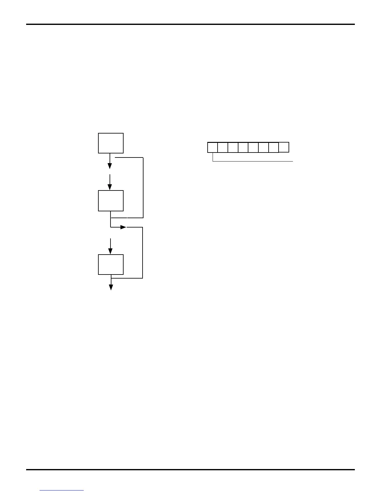
Figure 3-3. External Clock Circuit
÷2
OSC
External Clock
D1 (SMR)
÷16
D0 (SMR)
Figure 3-4. Port Configuration Register (PCON)
(Write-Only)
D7 D6 D5 D4 D3 D2 D1 D0
PCON (FH) 00H
Low EMI Oscillator
0 Low EMI
1 Standard