Z8 Microcontrollers
ZiLOG External Interface
UM001601-0803 10-7
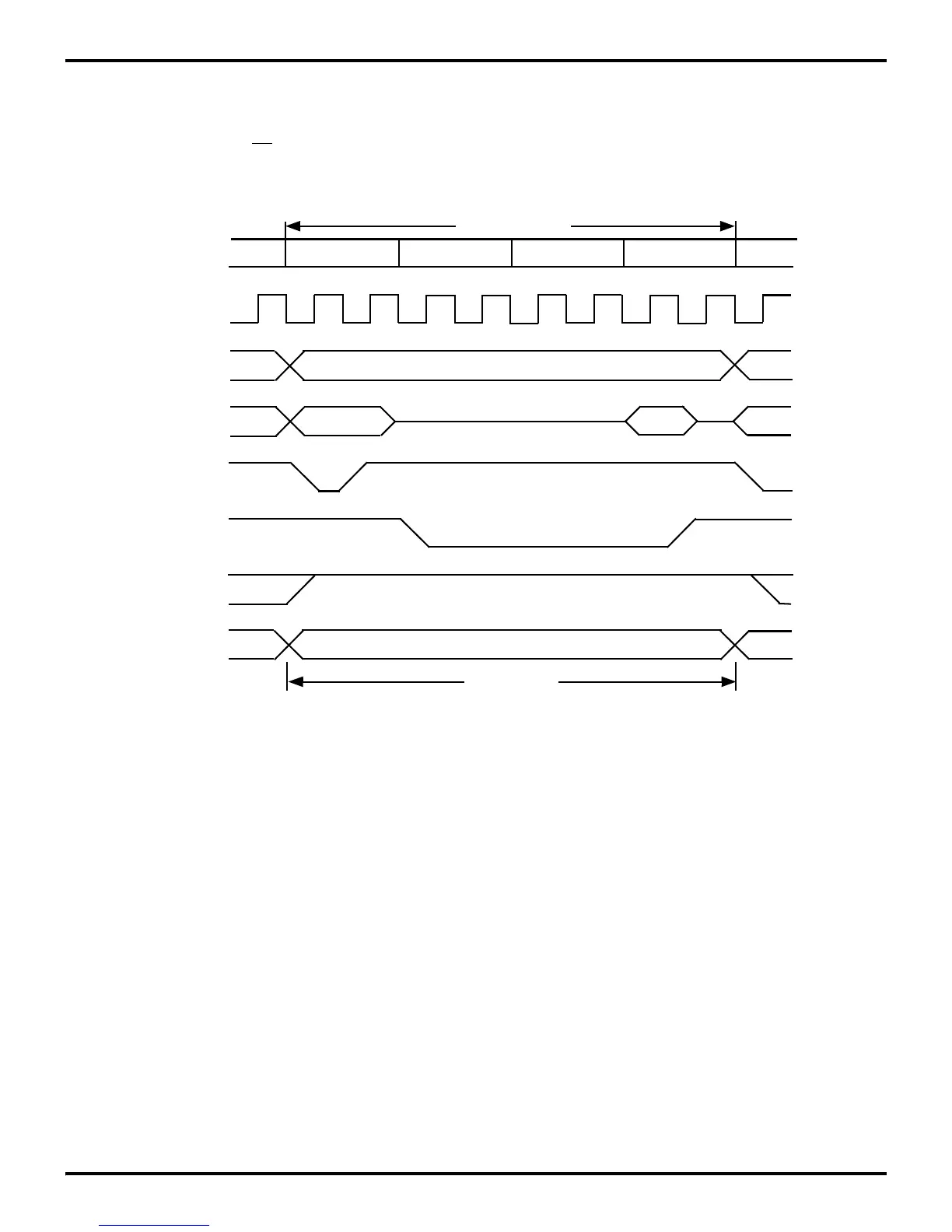
10.7 EXTENDED BUS TIMING
Some products can accommodate slow memory access time by
automatically inserting an additional software controlled state
time (Tx). This stretches the
DS timing by two clock periods.
Figures 10-7 and 10-8 illustrate extended external memory Read
and Write cycles.
Figure 10-7. Extended External Instruction Fetch or Memory Read Cycle
Machine Cycle
T2*
TX
T3
Clock
A15-A8
AD7-AD0
/AS
/DS
R/W
/DM
Read Cycle
A15-A8
A7-A0
D7-D0 IN
T1
*Port inputs are strobed during T2, which is two internal system clocks
before the execution of the current instruction.