UM001601-0803 3-1
USER’S MANUAL
CHAPTER 3
CLOCK
3.1 CLOCK
The Z8 MCU
®
derives its timing from on-board clock circuitry
connected to pins XTAL1 and XTAL2. The clock circuitry con
-
sists of an oscillator, a divide-by-two shaping circuit, and a clock
buffer. Figure 3-1 illustrates the clock circuitry. The oscillator’s
input is XTAL1 and its output is XTAL2. The clock can be driv
-
en by a crystal, a ceramic resonator, LC clock, RC, or an external
clock source.
3.1.1 Frequency Control
In some cases, the Z8 has an EPROM/OTP option or a Mask
ROM option bit to bypass the divide-by-two flip flop in Figure
3-1. This feature is used in conjunction with the low EMI option.
When low EMI is selected, the device output drive and oscillator
drive is reduced to approximately 25 percent of the standard
drive and the divide-by-two flip flop is bypassed such that the
XTAL clock frequency is equal to the internal system clock fre
-
quency. In this mode, the maximum frequency of the XTAL
clock is 4 MHz. Please refer to specific product specification for
availability of options and output drive characteristics.
3.2 CLOCK CONTROL
In some cases, the Z8 offers software control of the internal sys-
tem clock via programming register bits. The bits are located in
the Stop-Mode Recovery Register in Expanded Register File
Bank F, Register 0BH. This register selects the clock divide val
-
ue and determines the mode of Stop-Mode Recovery (Figure 3-
2). Please refer to the specific product specification for availabil
-
ity of this feature/register.
3.2.1 SCLK/TCLK Divide-By-16 Select (D0)
This bit of the SMR controls a divide-by-16 prescalar of
SCLK/TCLK. The purpose of this control is to selectively reduce
device power consumption during normal processor execution
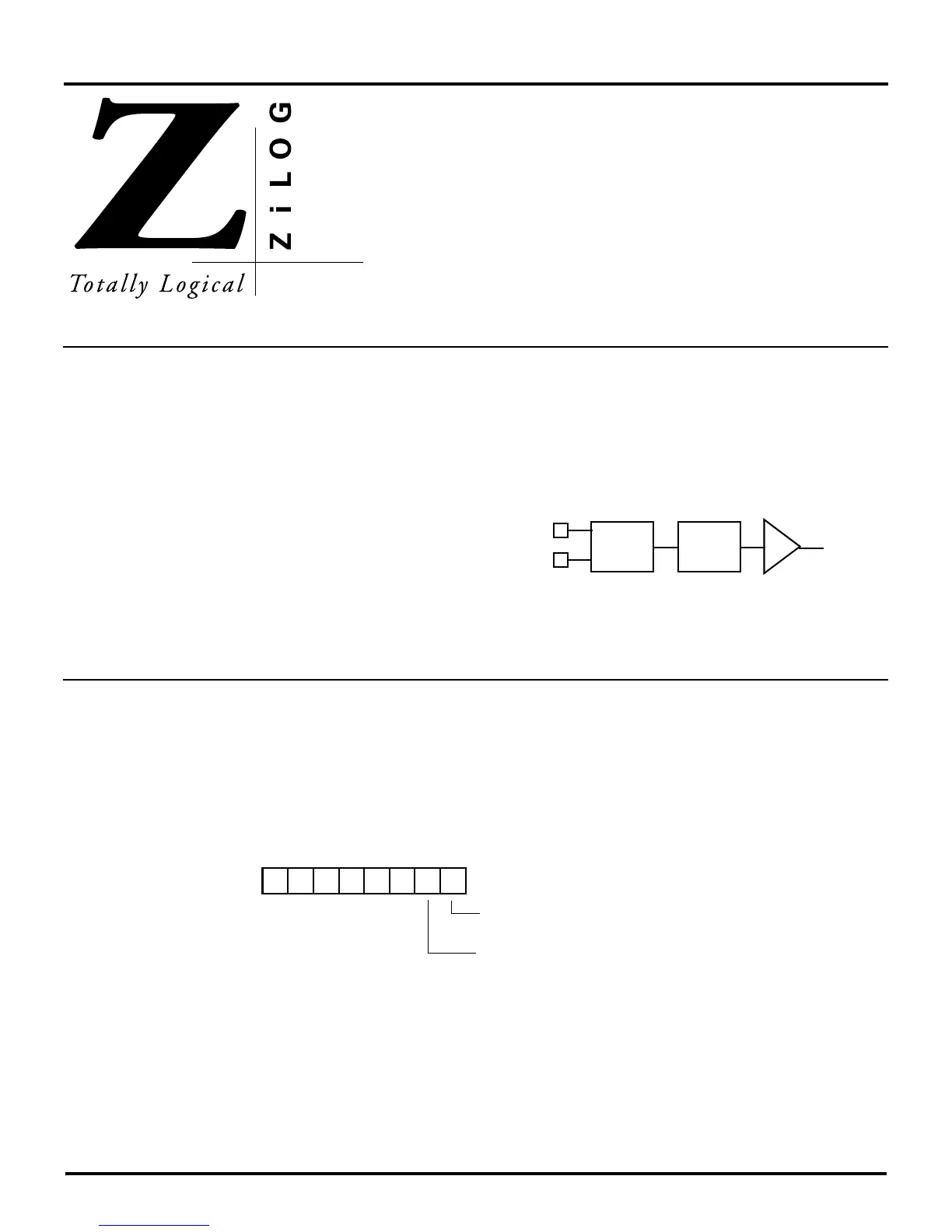
Figure 3-1. Z8 Clock Circuit
÷2
OSC
XTAL2
Internal
Buffer
XTAL1
Clock
Figure 3-2. Stop-Mode Recovery Register
(Write-Only Except D7, Which is Read-Only)
D7 D6 D5 D4 D3 D2 D1 D0
SMR (F) OB
SCLK/TCLK Divide by 16
0 OFF **
1 ON
External Clock Divide Mode by 2
0 = SCLK/TCLK = XTAL/2*
1 = SCLK/TCLK = XTAL
* Default setting after RESET.
**Default setting after RESET and STOP-Mode Recovery.

 Loading...
