Z8 Microcontrollers
Clock ZiLOG
3-4 UM001601-0803
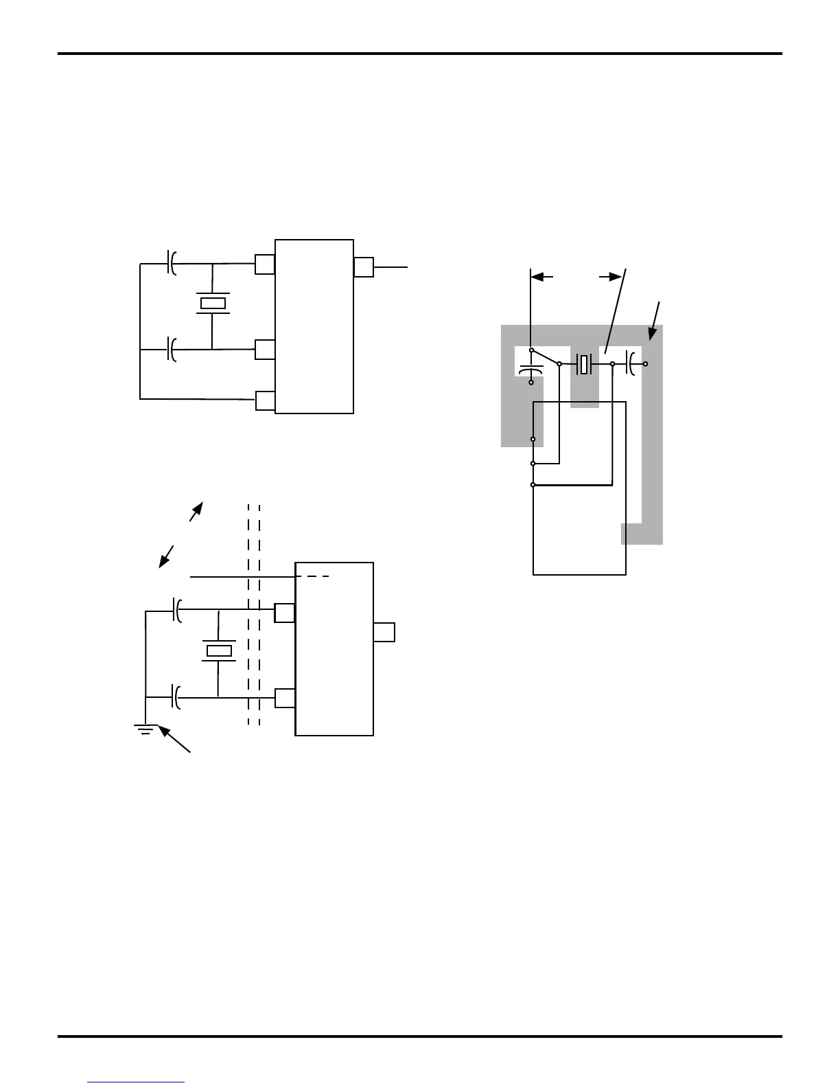
3.4.3 Circuit Board Design Rules
The following circuit board design rules are suggested:
• To prevent induced noise the crystal and load capacitors
should be physically located as close to the Z8® as possible.
• Signal lines should not run parallel to the clock oscillator
inputs. In particular, the crystal input circuitry and the internal
system clock output should be separated as much as possible.
•V
CC
power lines should be separated from the clock oscillator
input circuitry.
• Resistivity between XTAL1 or XTAL2 and the other pins
should be greater than 10 Mohms.
Figure 3-6. Circuit Board Design Rules
XTAL2
V
SS
XTAL1
Board Design Example
V
SS
2
3
1
Layout Should
Avoid High
Lighted Areas
Signal Line
20 mm
max
Z8
Z8
Z8
C1
C2
3
2
Clock Generator Circuit
Signals A B
Signal C
(Connection to System Group
Must Be Avoided)
(Parallel Traces
Must Be Avoided)
(Top View)