Z8 Microcontrollers
ZiLOG I/O Ports
UM001601-0803 5-5
5.3 PORT 1
This section deals only with the I/0 operation. The port's external
memory interface operation is discussed later in this manual.
Figure 5-2 shows a block diagram of Port 1.
5.3.1 General I/O Mode
Port 1 can be an 8-bit, bidirectional, CMOS or TTL compatible
port with multiplexed Address (A7–A0) and Data (D7–D0)
ports. These eight I/O lines can be byte programmed as inputs or
outputs or can be configured under software control as an Ad
-
dress/Data port for interfacing to external memory. The input
buffers can be Schmitt-triggered, level- shifted, or a single-point
buffer. In some cases, the output buffers can be globally pro
-
grammed as either push-pull or open-drain. Low-EMI output
buffers can be globally programmed by software, as an OTP pro
-
gram option, or as a ROM Mask Option. In some cases, the
Z8can have auto latches hardwired to the inputs. Please refer to
specific product specifications for exact input/output buffer-type
features available (Figures 5-7 and 5-8).
Figure 5-5. Port 0 I/O Operation
Figure 5-6. Port 0 Handshake Operation
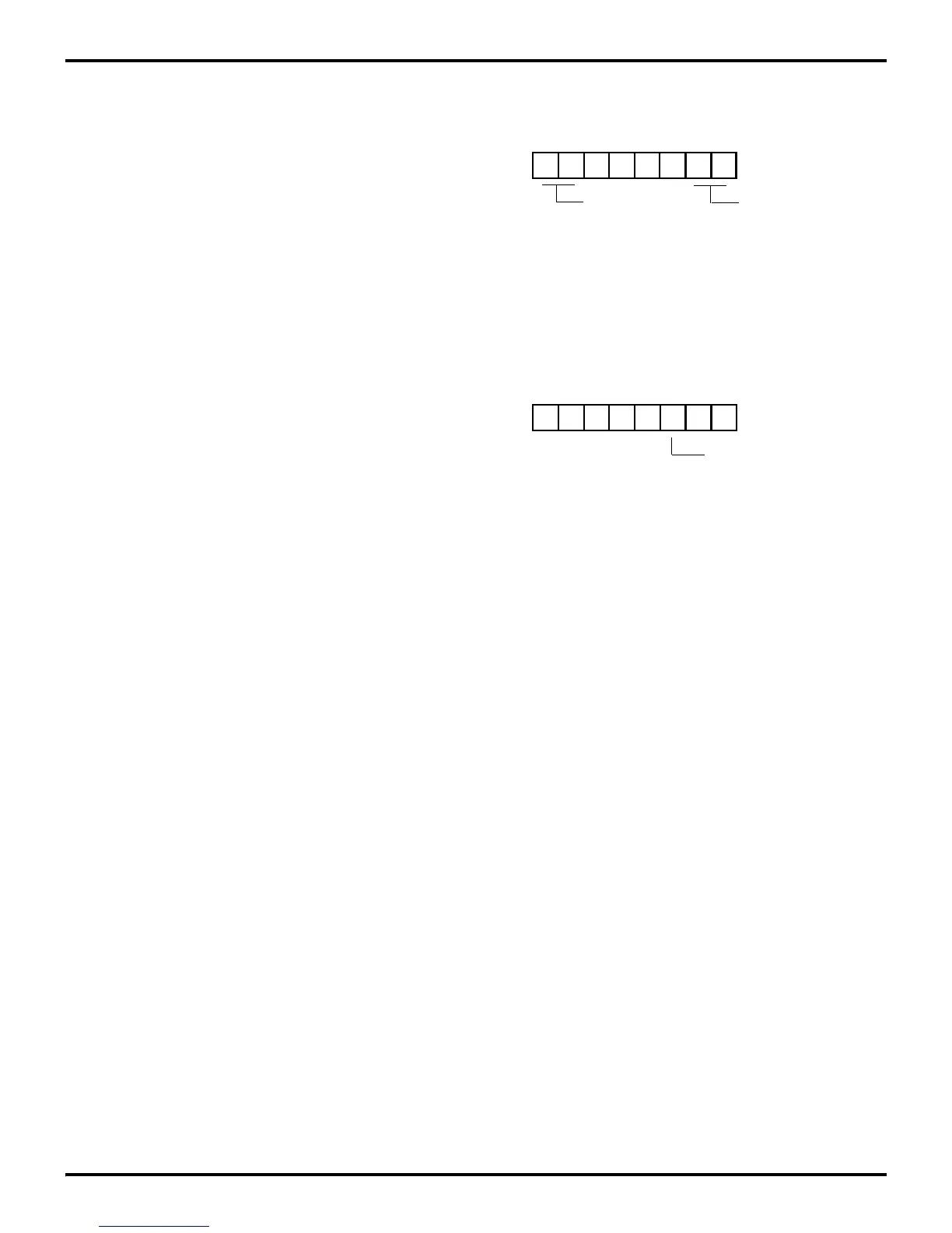
D7 D6 D1 D0
(Write-Only)
01 = Input
1X = A
8
- A
11
P0
0
- P0
3
Mode
00 = Output
Port 0-1 Mode Register (P01M)
Register F8H (P01M)
P0
4
- P0
7
Mode
00 = Output
01 = Input
1X = A
12
- A
15
D2
(Write-Only)
0 P3
2
= Input
P3
5
= Output
Port 3 Mode Register (P3M)
Register F7H
1 P3
2
= DAV0/RDY0
P3
5
= RDY0/DAV0

 Loading...
