Z8 Microcontrollers
ZiLOG I/O Ports
UM001601-0803 5-31
Auto Latch Model:
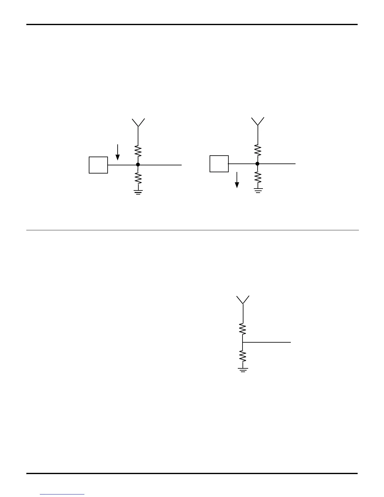
The Auto Latch’s equivalent circuit is shown in Figure 5-39.
When the input is high, the circuit consists of a resistance Rp
from V
DD
(the P-channel transistor in its ON state) and a much
greater resistance Rh to G
ND
. Current Iao flows from V
DD
to the
output. When the input is low, the circuit may be modeled as a
resistance Rp from G
ND
(the N-channel transistor in the ON
state) and a much greater resistance Rh to V
DD
. Current Iao now
flows from the input to ground. The Auto Latch is characterized
with respect to Iao, so the equivalent resistance Rp is calculated
according to R
P
= (V
DD
-VIN)/I
AO
. The worst case equivalent re-
sistance Rp (min) may be calculated at the worst case input volt-
age, V
I
= V
IH
(min).
Design Considerations:
For circuits in which the Auto Latch is active, consideration
should be given to the loading constraints of the Auto Latches.
For example, with weak values of V
IN
, close to Vih (min) or Vil
(max), pullup or pull-down resistances must be calculated using
Ref = R/Rp. For best case STOP mode operation, the inputs
should be within 200 mV of the supply rails.
In output mode, if a port bit is forced into a tri-state condition,
the Auto Latches will force the pad to V
DD
. If there is an external
pulldown resistor on the pin, the voltage at the pin may not
switch to GND due to the Auto Latch. As shown in Figure 5-40,
the equivalent resistance of the Auto Latch and the external pull
-
down form a voltage divider, and if the external resistor is large,
the voltage developed across it will exceed Vil(max). For worst
case:
V
IL
(max > V
DD
[Rext/(Rext+Rp)]
Rext(max) = [(Vil(max)/V
DD
)Rp]/[1-(Vil(max)/V
DD
)]
For V
DD
= 5.0V and Iao = 5 uA we have Vih(max) =0.8V:
R
EXT
(max) = (0.16/1M)/(1–0.16) = 190 K ohms.
Rp increases rapidly with V
DD
, so increased V
DD
will relax the
requirement on Rext.
In summary, the CMOS Z8 Auto Latch inhibits excessive cur-
rent drain in Z8 devices by latching an open input to either V
DD
or GND. The effect of the Auto Latch on the I/O characteristics
of the device may be modeled by a current Iao and a resistor Rp,
whose value is V
DD
/Iao.
Figure 5-39. Auto Latch Equivalent Circuit
V
DD
Data in
PIN
Logic 1
A0
PIN
V
DD
R
P
R
H
R
H
R
P
Data in
Logic 0
A0
Figure 5-40. Effect of Pulldown Resistors on Auto Latches
V
LO
V
IH
(min.)
R
P
R
EXT
 Loading...

