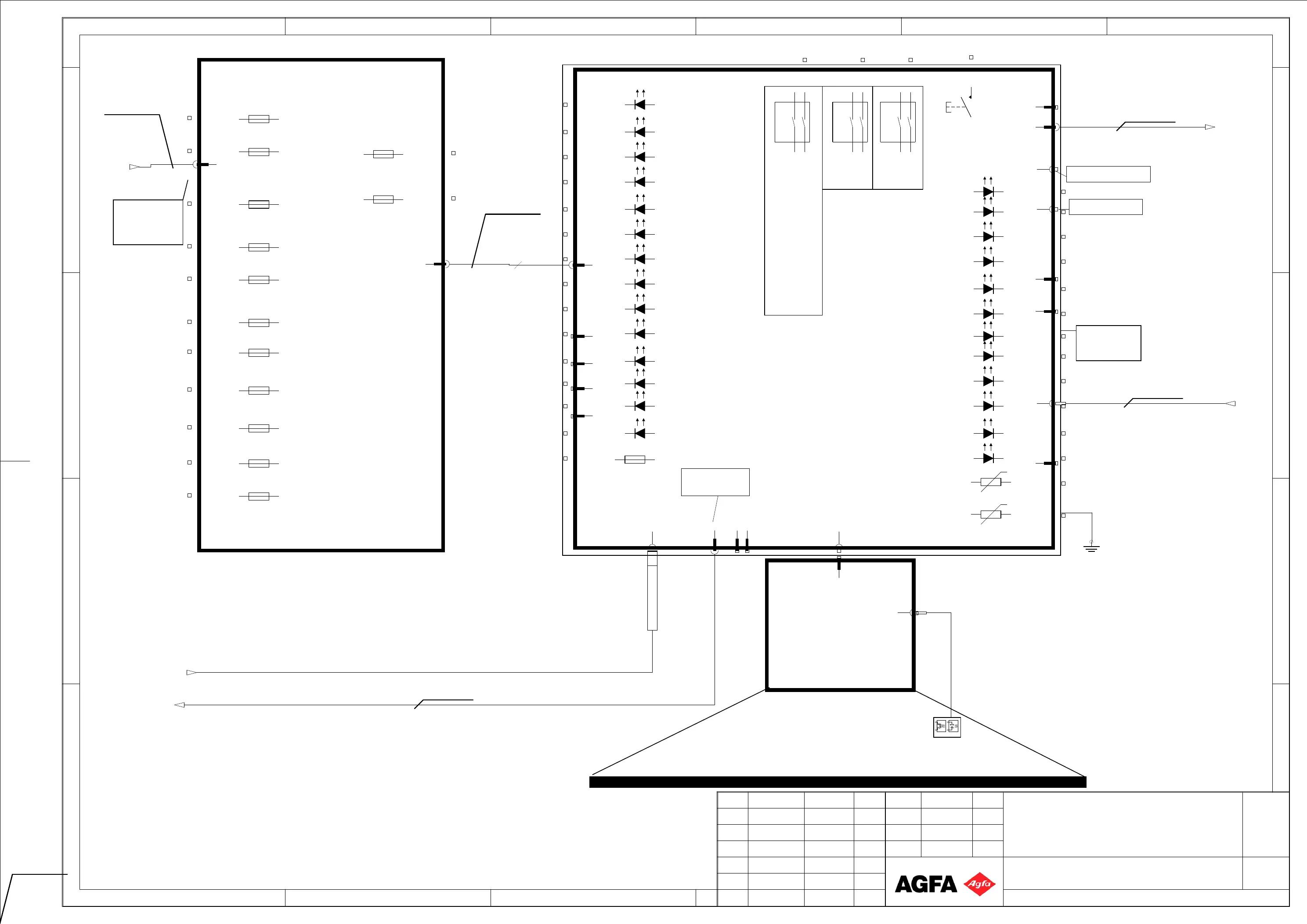
4991.DFB
-B410
F7-5170-4981-0.dfb
-B411
-B422
-P24
*4/4
DIL-SWITCH
OFF
-S1
-S2
-LD30
-LD31
-LD32
-LD33
-LD34
-LD35
-LD36
-LD37
-LD38
-LD39
-LD40
-LD41
-LD42
-LD43
-LD44
DIL-SWITCH
OFF
-S3
DIL-SWITCH
OFF
-S4
-LD2
-LD48
-LD50
-LD51
-LD52
-BU1#10
*4/4
-P2#11
*6/6
-R1229
-LD53
-P34
*10/10
-L1#12
-L2#12
F7.0471.9202.0
-P36
*50/50
-P1#5
*9/9
-F1#5
-R1#12
-P17
#25/26
F7.0471.9196.0
-P25
*17/17
-LD45
-LD47
S/11
S/11
-LD46
-P16
*9/9
-F17
-F18
-F19
-F23
-F24
-F25
F7.0471.9202.0
-P5
*50/50
-F27
F7.0429.0038.0
-P3
*8/8
-F13
-F15
-F16
-F1#1
-F1
-F20
-BU1
+B422
+B422
/FRAME.4F
#14073
/Cassette_Unit.3A
/Scanner_Unit.2A
X
/Scan_Modul.1F
X
/FRAME.1E
/FRAME.4F
#13127
/Scanner_Unit.1F
X
-BU129
*8/8
F7.0471.8924.0
-BU133
#9/10
L7.0472.1012.0
-BU177
*50/50
L7.0472.1012.0
-BU178
*50/50
-BU176
#25/26
P323326
-ST23
-W960:B *6
F7.0471.8670.0
-ST17
#9/10
-ST34
-P22
*80/80
-P21
*80/80
-P1#6
#9/11
-P1
*10/10
A B C D E F
A B C
4
3
2
1
3
2
1
/
IDX Change-NR DATE NAME Replacement for
Sheet
of SH
Project
DATE NAME
USER
APPR.
NORM
We reserve all rights in this document and in the information
contained therein. Reproduction, use or disclosure to
third parties without explicit authorisation is strictly forbidden.
© AGFA
Sheet name:
4
03.01.2006 Leith.
F1.5175.8503.0
37407
38631
39319
5175
100
CR30-X
General Schematic
0A
0B
20.04.06
31.05.06
29.08.06
Leith.
Leith.
Leith.
9
4
Light_Collector
-P30
*10/10
-ST1#1
*10/10
-P17
S/26
-W924_1
F8.5175.8540.0
-W906
F8.5175.8550.0
F8.5175.8510.0
F8.5175.8535.0A
-W1070
-W1071
F7.5175.8515.0
#50
PMI-BOARD
DISTRIBUTION-BOARD
PMI_POWER-
Light collector
EMI-BOX for
Program and test connectors
Test connector
E-Label connector
ConF/FPGA done
M32 Reserve 2
M32 Reserve 1
FPGA Test 3
FPGA Test 4
M32 NCS 0
M32 NCS 1
M32 NCS 2
M32 NCS 3
M32 OPT + OK
M32 OPT - OK
M32 CAL + OK
M32 CAL - OK
V33_PHY#12
V33_PHY
FPGA NRESET
5.0VD
M32 PMT + OK
M32 PMT - OK
M32 Analog OK
M32 CAN OK
M32 LCD OK
M32 WDG
3,3VD
1,5VD
PMI-BOARD
resistor 121 Ohm
CAN-Terminating
from EOL/BOL Sensor Array
Supply on Bu129
tolerance limit + / - 5%
1,2,3,4= +24VDC
5,6,7,8 = GND
from Cassette Unit open Safety Switch
NC
RS232 Debug-Interface
F8.5175.2290.X
T1A
-10V PMT
T1A
+12V
F7A
T5A
24VDC
T2,5A
+12V OPT
T3,5A
1,5VD
T3,5A
3,3VD
T1A
+20V PMT
T1A
+20V PMT
T2,5A
+8V Disp.
T2,5A
-12V OPT
T1A
+8V Analog
T2A
Power Supply
Polygon Motor
F8.5170.4980.X
P1
PMT
F8.5175.3040.X
9pol. DSUB
Auto_Cal_LED
Reset
M32 Reserve 1
M32 Reserve 2
FPGA Test1
FPGA Test2
1,25A
+24.0V POL
300mA
5.0VD_FW
+24.0V POL
1-4 ON= Free Run Mode
1-4 OFF= Start Monitor
2-3 ON= Cfg.-EEPROM write protected
2-3 OFF= Cfg.-EEPROM not write protected
125mA
VCC_NODE
PWR_CAN
IN 24VDC


 To Next Page