A20 User Manual (Revision 1.2) Copyright © 2013 Allwinner Technology Co., Ltd. All Rights Reserved. Page 318 / 812
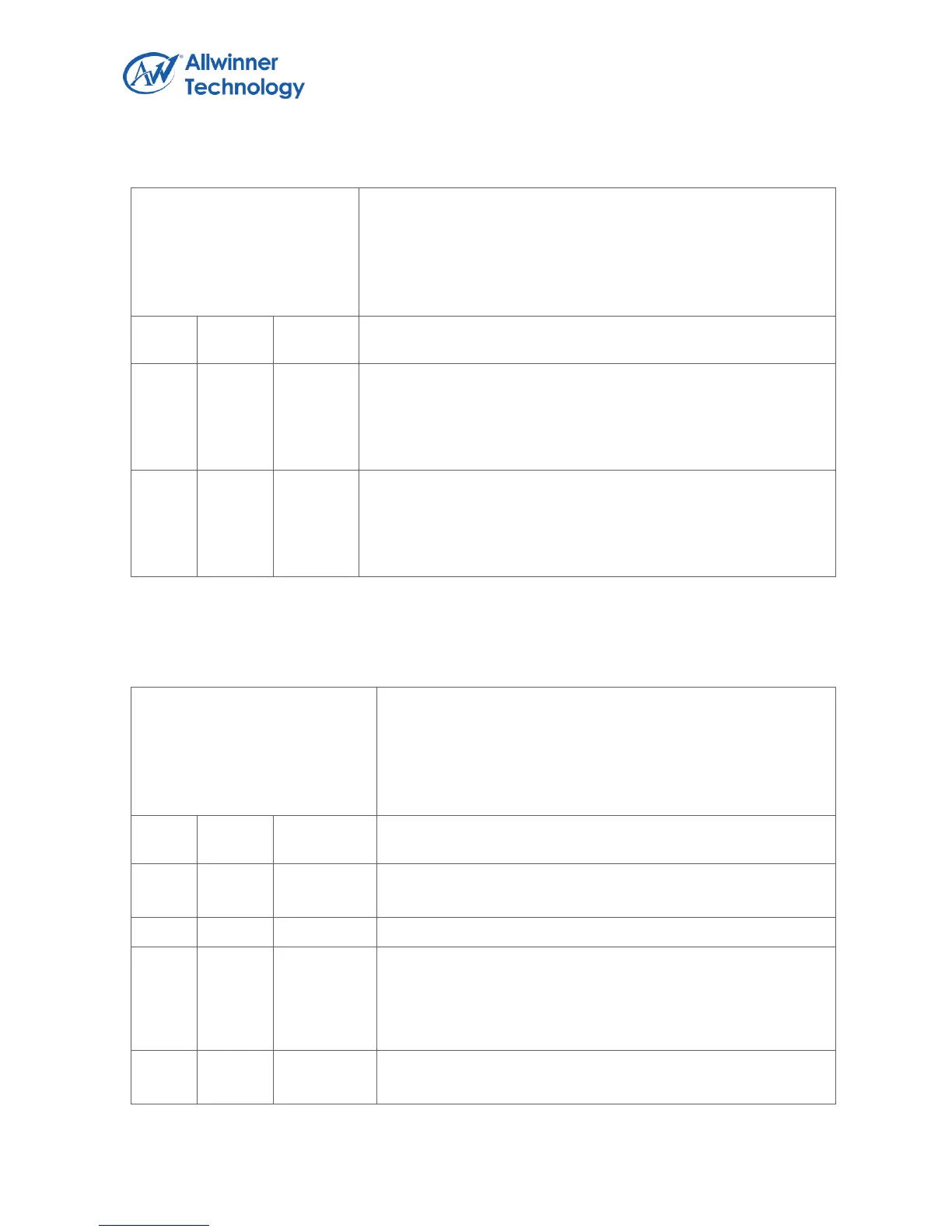
3.1.4.8. INPUT DMA MEMORY BLOCK COORDINATE CONTROL REGISTER
Offset:
iDMA0:0x40
iDMA1:0x44
iDMA2:0x48
iDMA3:0x4C
Register Name: MP_IDMACOOR_REG
IDMA_YCOOR
Y coordinate
Y is the left-top y coordinate of layer on output window in pixels
The Y represent the two’s complement
IDMA_XCOOR
X coordinate
X is left-top x coordinate of the layer on output window in pixels
The X represent the two’s complement
3.1.4.9. INPUT DMA SETTING REGISTER
Offset:
iDMA0:0x50
iDMA1:0x54
iDMA2:0x58
iDMA3:0x5C
Register Name: MP_IDMASET_REG
IDMA_GLBALPHA
Globe alpha value
IDMA_FCMODEN
Fill color mode enable control
0: disable
1: enable
IDMA_PS
Input data pixel sequence
 Loading...