A20 User Manual (Revision 1.2) Copyright © 2013 Allwinner Technology Co., Ltd. All Rights Reserved. Page 508 / 812
5.3.4.51. DEFE_3D_BUF_ADDR1_REG
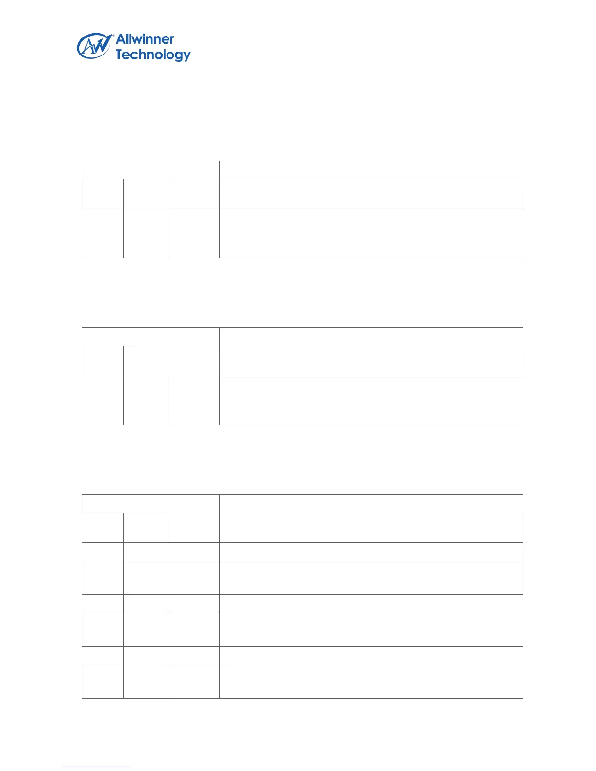
Register Name: DEFE_3D_BUF_ADDR1_REG
RIGHT_CH1_ADDR
3D mode channel 1 buffer address
This address is the start address of right image in 3D mode
5.3.4.52. DEFE_3D_BUF_ADDR2_REG
Register Name: DEFE_3D_BUF_ADDR2_REG
RIGHT_CH2_ADDR
3D mode channel 2 buffer address
This address is the start address of right image in 3D mode
5.3.4.53. DEFE_3D_TB_OFF0_REG
Register Name: DEFE_3D_ TB_OFF0_REG
X_OFFSET1
The x offset of the bottom-right point in the first tile
Y_OFFSET0
The y offset of the top-left point in the first tile
X_OFFSET0
The x offset of the top-left point in the first tile
 Loading...