A20 User Manual (Revision 1.2) Copyright © 2013 Allwinner Technology Co., Ltd. All Rights Reserved. Page 782 / 812
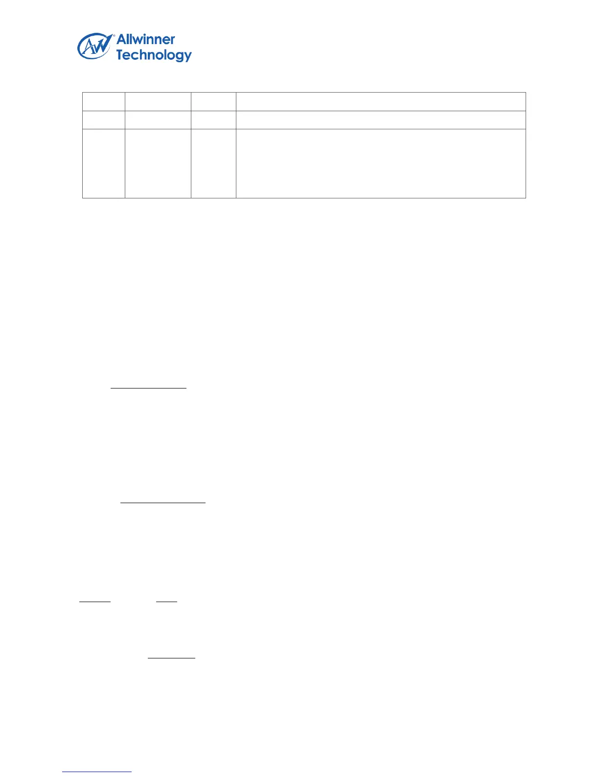
FIFO_DATA
This 8-bit register provides access to the RX and TX FIFO
buffers. The TX FIFO is accessed during the APB write
transfer. The RX FIFO is accessed during the APB read
transfer.
6.14.6.
Smart Card Reader Special Requirement
CLOCK GENERATOR
The Clock Generator generates the Smart Card Clock signal and the Baud Clock Impulse signal, used in
timing the Smart Card Reader.
The Smart Card Clock signal is used as the main clock for the smart card. Its frequency can be adjusted
using the Smart Card Clock Divisor (SCCDIV). This value is used to divide the system clock. The SCCLK
frequency is given by the following equation:
2 * ( 1)
sysc lk
scclk
f
f
SC C D IV
-- Smart Card Clock Frequency
-- System Clock (PCLK) Frequency
The Baud Clock Impulse signal is used to transmit and receive serial between the Smart Card Reader and
the Smart Card. The baud rate can be modified using the Baud Clock Divisor (BAUDDIV). The value is
used to divide the system clock. The BUAD rate is given by the following equation:
2 * ( 1)
sysc lk
f
B A U D
B A U D D IV
-- Baud rate of the data stream between Smart Card and Reader
The duration of one bit, Elementary Time Unit (ETU), is defined in the ISO/IEC 7816-3 specification.
During the first answer to reset response after the cold reset, the initial ETU must be equal to 372 Smart
Card Clock Cycles.
1 37 2
scclk
E T U
B A U D f
In this case, the BAUDDIV should be
.
37 2 *
1 3 72 * ( 1) 1
2*
sysclk
scclk
f
B A U D D IV S C C D IV
f
After the ATR is completed, the ETU can be changed according to Smart Card abilities.
 Loading...