System Control
ARM DDI 0500D Copyright © 2013-2014 ARM. All rights reserved. 4-234
ID021414 Non-Confidential
Used in conjunction with VTTBR, that defines the translation table base
address for the translations.
Configurations VTCR is architecturally mapped to AArch64 register VTCR_EL2. See
Virtualization Translation Control Register, EL2 on page 4-91.
This register is accessible only at EL2 or EL3.
Attributes VTCR is a 32-bit register.
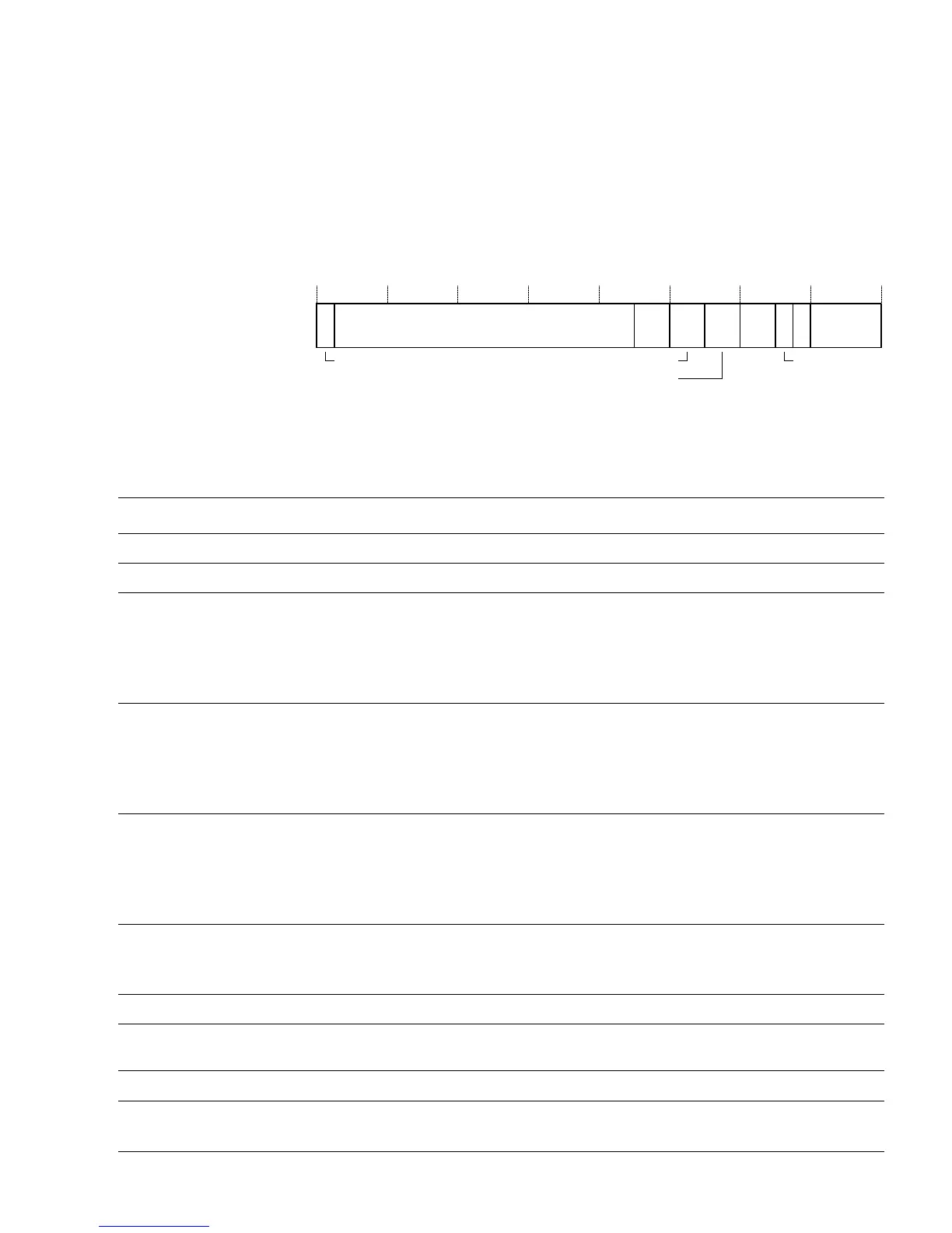
Figure 4-118 shows the VTCR bit assignments.
Figure 4-118 VTCR bit assignments
Table 4-213 shows the VTCR bit assignments.
To access the VTCR:
Table 4-213 VTCR bit assignments
Bits Name Function
[31] - Reserved,
RES1.
[30:14] - Reserved,
RES0.
[13:12] SH0 Shareability attribute for memory associated with translation table walks using TTBR0.
0b00
Non-shareable.
0b01
Reserved.
0b10
Outer Shareable.
0b11
Inner Shareable.
[11:10] ORGN0 Outer cacheability attribute for memory associated with translation table walks using TTBR0.
0b00
Normal memory, Outer Non-cacheable.
0b01
Normal memory, Outer Write-Back Write-Allocate Cacheable.
0b10
Normal memory, Outer Write-Through Cacheable.
0b11
Normal memory, Outer Write-Back no Write-Allocate Cacheable.
[9:8] IRGN0 Inner cacheability attribute for memory associated with translation table walks using TTBR0.
0b00
Normal memory, Inner Non-cacheable.
0b01
Normal memory, Inner Write-Back Write-Allocate Cacheable.
0b10
Normal memory, Inner Write-Through Cacheable.
0b11
Normal memory, Inner Write-Back no Write-Allocate Cacheable.
[7:6] SL0 Starting level for translation table walks using VTTBR:
0b00
Start at second level.
0b01
Start at first level.
[5] - Reserved,
RES0.
[4] S Sign extension bit. This bit must be programmed to the value of T0SZ[3]. If it is not, then the stage 2 T0SZ value
is treated as an
UNKNOWN value within the legal range that can be programmed.
[3:0] T0SZ
The size offset of the memory region addressed by TTBR0. The region size is 2
32-T0SZ
bytes.