6-5
6 I/O Memory Areas
CJ2 CPU Unit Software User’s Manual
6-1 I/O Memory Areas
6
6-1-2 I/O Memory Area Structure
• Serial Communications Units: CJ1W-SCU22, CJ1W-SCU32, and CJ1W-SCU42
*7 Index registers and data registers can be used either individually by task or they can be shared by all the tasks.
*8 Banks D to 18 hex of the EM Area were added to expand the EM Area in CJ2 CPU Units. Also, the ability to address bits
in the DM Area and EM Area was also added as a new feature to the CJ2 CPU Units.
Banks D to 18 hex of the EM Area cannot be accessed and bit addresses in the DM Area and EM Area cannot be used by
CPU Bus Units, Special I/O Units, PTs, and Support Software that do not specifically support the CJ2 CPU Units.
Only the following CPU Bus Units and Special I/O Units specifically support the CJ2 CPU Units.
• EtherNet/IP Unit: CJ1W-EIP21
• Position Control Units: CJ1W-NC214, CJ1W-NC234, CJ1W-/NC281, CJ1W-NC414, CJ1W-NC434,
CJ1W-NC481, and CJ1W-NC881
• Analog Input Unit: CJ1W-AD042
• Analog Output Unit: CJ1W-DA042V
• Serial Communications Units: CJ1W-SCU22, CJ1W-SCU32, and CJ1W-SCU42
*9 Bits in the specified bank and all banks after it can be force-set/reset. (This is called the EM Area force-set/reset function.)
With CJ2H CPU Units, bits in following EM Area banks that are set for automatic address allocation can be force-
set/reset.
CJ2H-CPU64/65(-EIP): E03_0 to E03_32767
CJ2H-CPU65(-EIP): E06_0 to E09_32767
CJ2H-CPU67(-EIP): E07_0 to E0E_32767
CJ2H-CPU68(-EIP): E11_0 to E18_32767
*10 Timer PVs can be refreshed indirectly by force-setting/resetting Timer Completion Flags.
*11 Counter PVs can be refreshed indirectly by force-setting/resetting Counter Completion Flags.
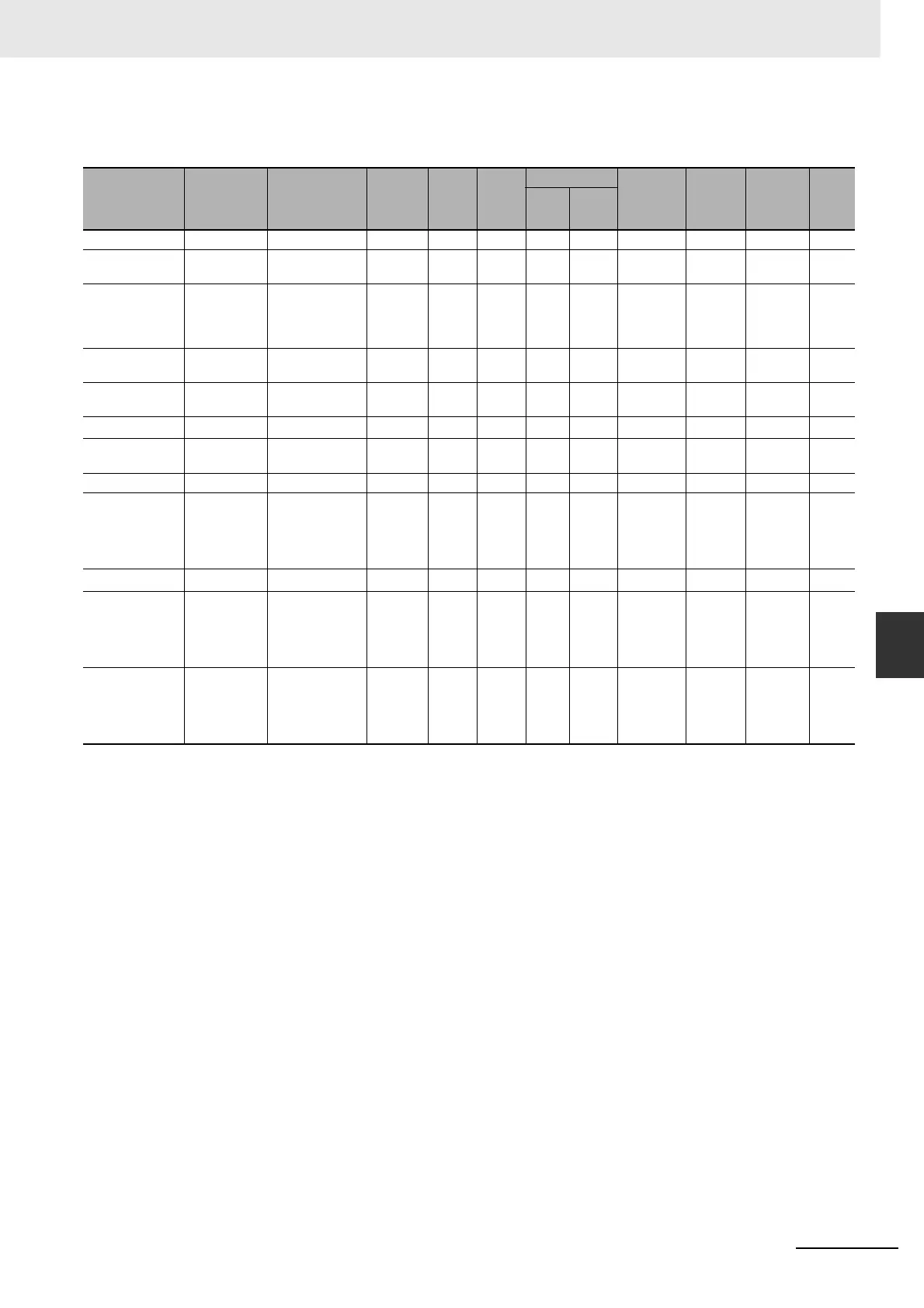
Area Size Range
External
I/O allo-
cation
Bit
access
Word
access
Access Change
from Pro-
gramming
Device
Status at
startup
or mode
change
Forcing
bit status
Refer-
ence
Read Write
TR Area 16 bits TR0 to TR15 --- OK --- OK OK No Cleared No 6-24
DM Area 32,768 words D00000 to
D32767
---
OK
*8
OK OK OK OK Main-
tained
No 6-25
EM Area 32,768 words
per bank, 25
banks max. (0
to 18 hex)
E00_0 to
E18_32767
*8
---
OK
*8
OK OK OK OK Main-
tained
Can be
enabled
with a set-
ting.
*9
6-28
Timer Completion
Flags
4,096 bits T0 to T4095 --- OK --- OK OK OK Cleared OK 6-32
Counter Comple-
tion Flags
4,096 bits C0 to C4095 --- OK --- OK OK OK Main-
tained
OK 6-34
Timer PVs 4,096 words T0 to T4095 --- --- OK OK OK OK Cleared
No
*10
6-32
Counter PVs 4,096 words C0 to C4095 --- --- OK OK OK OK Main-
tained
No
*11
6-34
Task Flag Area 128 bits TK000 to TK127 --- OK --- OK No No Cleared No 6-35
Index Registers
*7
16 registers IR0 to IR15 --- OK OK Indi-
rect
addre
ssing
only
Spe-
cific
instruct
ions
only
No Cleared No 6-36
Data Registers
*7
16 registers DR0 to DR15 --- No OK OK OK No Cleared No 6-41
Condition Flags Example:
Always ON
Flag
System symbols
in the global sym-
bols table of the
CX-Programmer
(e.g., P_On)
--- OK --- OK No No Cleared No 6-43
Pulse bits Example: 1 s
Clock Pulse
System symbols
in the global sym-
bols table of the
CX-Programmer
(e.g., P_1s)
--- OK --- OK No No Cleared No 6-45