Section 25 Electrical Characteristics
Rev. 4.00 Sep. 14, 2005 Page 957 of 982
REJ09B0023-0400
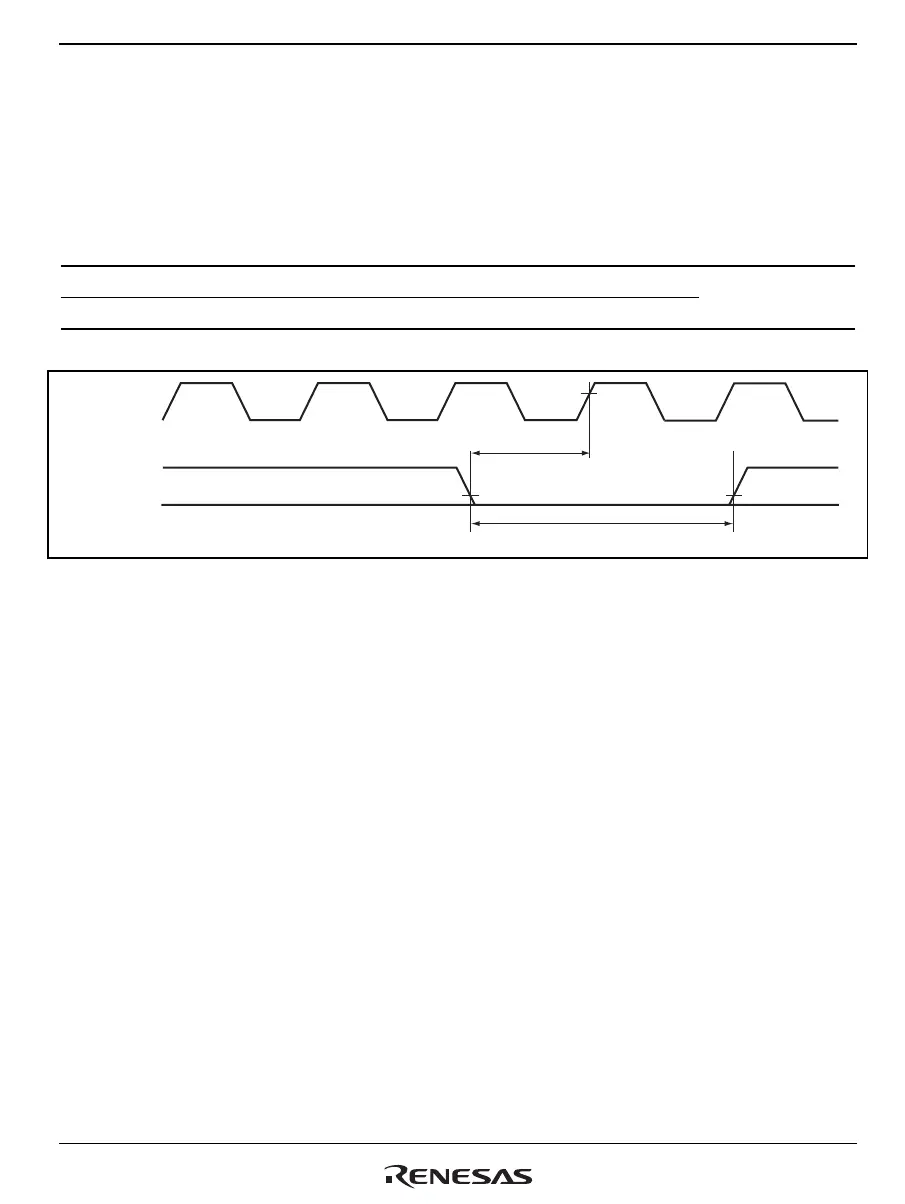
25.3.10 POE Module Signal Timing
Table 25.11 Output Enable (POE) Timing
Conditions: V
CC
= 1.8 V ± 5%, V
CC
Q = AV
CC
= 3.0 V to 3.6 V, V
SS
= V
SS
Q = AV
SS
= 0 V,
Ta = −40°C to +85°C
Item Symbol Min. Max. Unit Figure(s)
POE input setup time t
POES
B
cyc
/2+10 — ns 25.49
POE input pulse width t
POEW
1.5 — t
pcyc
CKIO
POEn input
t
POES
t
POEW
Figure 25.49 POE Input/Output Timing