Section 18 Multi-Function Timer Pulse Unit (MTU)
Rev. 4.00 Sep. 14, 2005 Page 593 of 982
REJ09B0023-0400
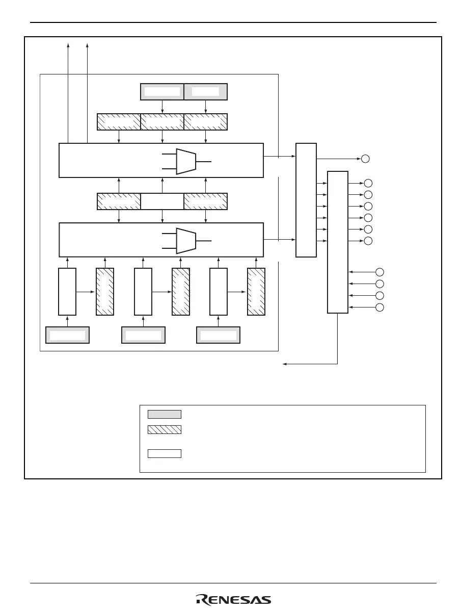
TGRC_3
TDDR
TCNT_3
TGRD_3 TGRD_4TGRC_4
TGRB_3
Temp 1
TGRA_4
Temp 2
TGRB_4
Temp 3
TCNTS TCNT_4
TGRA_3 TCDR
TCBR
Comparator
Comparator
Match
signal
Match
signal
Output controller
Output protection circuit
PWM cycle
output
PWM output 1
PWM output 2
PWM output 3
PWM output 4
PWM output 5
PWM output 6
POE0
POE1
POE2
POE3
External cutoff
input
External cutoff
interrupt
: Registers that can always be read or written from the CPU
: Registers that cannot be read or written from the CPU
(except for TCNTS, which can only be read)
: Registers that can be read or written from the CPU
(but for which access disabling can be set by port E)
TGRA_3 compare-
match interrupt
TCNT_4 underflow
interrupt
Figure 18.32 Block Diagram of Channels 3 and 4 in Complementary PWM Mode
 Loading...


