38 CHAPTER 1 Introduction
J-Link / J-Trace (UM08001) ©
2004-2017 SEGGER Microcontroller GmbH & Co. KG
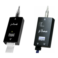
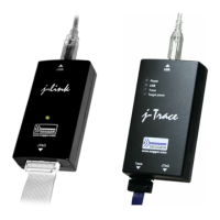
1.3.4.3 Hardware versions
Version 1.1
Compatible to J-Link.
• Initial design based on ATMEL SAM3U without FPGA.
Version 4
• New design based on STM32F407 + FPGA (Cyclone IV)Version 4.3
Identical to version 4 with the following exception:
Pin 1 (VTref) is used for measuring target reference voltage only. Buffers on J-Link
side are no longer powered through this pin but via the J-Link internal voltage sup-
plied via USB.
1.3.4.4 Software and Hardware Features Overview
For detailed information about hardware and software features of your J-Link/J-Trace
model and version see:
https://wiki.segger.com/Software_and_Hardware_Features_Overview
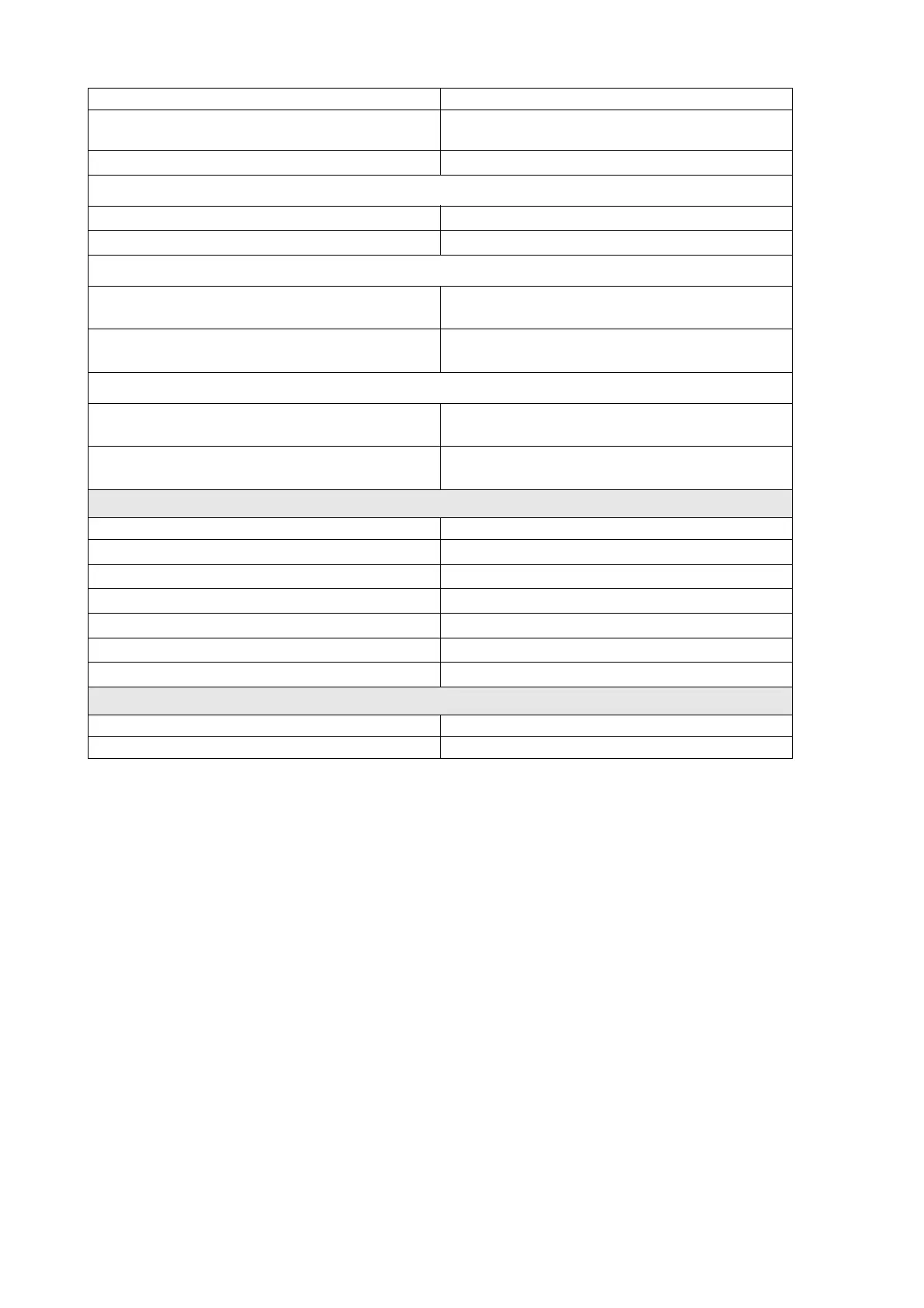
Target supply current Max. 300mA
Reset Type
Open drain. Can be pulled low or
tristated.
Reset low level output voltage (V
OL
)V
OL
<= 10% of V
IF
For the whole target voltage range (1.8V <= V
IF
<= 5V)
LOW level input voltage (V
IL
)V
IL
<= 40% of V
IF
HIGH level input voltage (V
IH
)V
IH
>= 60% of V
IF
For 1.8V <= V
IF
<= 3.6V
LOW level output voltage (V
OL
) with a
load of 10 kOhm
V
OL
<= 10% of V
IF
HIGH level output voltage (V
OH
) with a
load of 10 kOhm
V
OH
>= 90% of V
IF
For 3.6 <= V
IF
<= 5V
LOW level output voltage (V
OL
) with a
load of 10 kOhm
V
OL
<= 20% of V
IF
HIGH level output voltage (V
OH
) with a
load of 10 kOhm
V
OH
>= 80% of V
IF
JTAG/SWD Interface, Timing
SWO sampling frequency Max. 100 MHz
Data input rise time (T
rdi
)T
rdi
<= 20ns
Data input fall time (T
fdi
)T
fdi
<= 20ns
Data output rise time (T
rdo
)T
rdo
<= 10ns
Data output fall time (T
fdo
)T
fdo
<= 10ns
Clock rise time (T
rc
)T
rc
<= 3ns
Clock fall time (T
fc
)T
fc
<= 3ns
Analog power measurement interface
Sampling frequency 50 kHz
Resolution 1 mA
Table 1.3: J-link ULTRA specifications