J-Link / J-Trace (UM08001) © 2004-2017 SEGGER Microcontroller GmbH & Co. KG
421
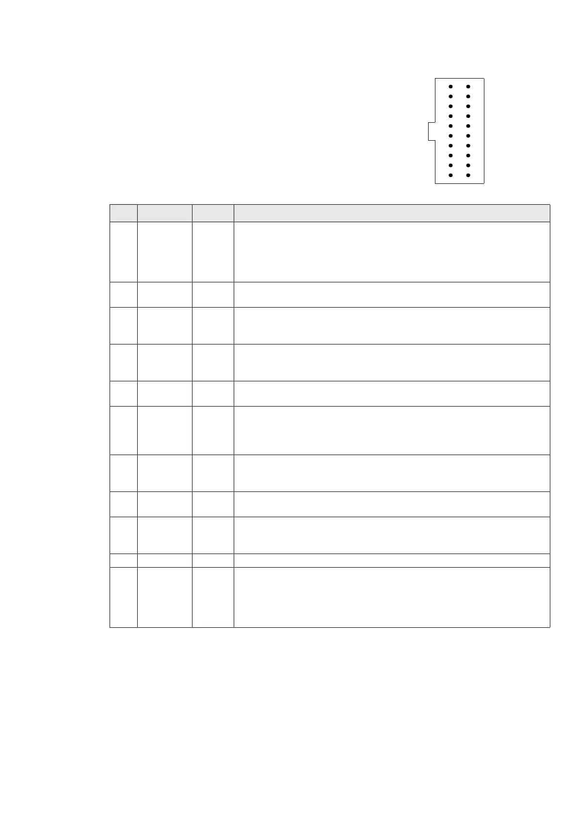
16.1.2 Pinout for SWD
The J-Link and J-Trace JTAG connector is also com-
patible to ARM’s Serial Wire Debug (SWD).
*On later J-Link products like the J-link ULTRA,
these pins are reserved for firmware extension pur-
poses. They can be left open or connected to GND in
normal debug environment. They are not essential
for JTAG/SWD in general.
The following table lists the J-Link / J-Trace SWD
pinout.
Pins 4, 6, 8, 10, 12, 14, 16, 18, 20 are GND pins connected to GND in J-Link. They
should also be connected to GND in the target system.
PIN SIGNAL TYPE Description
1VTref Input
This is the target reference voltage. It is used to check if
the target has power, to create the logic-level reference for
the input comparators and to control the output logic levels
to the target. It is normally fed from Vdd of the target board
and must not have a series resistor.
2
Not con-
nected
NC This pin is not connected in J-Link.
3Not UsedNC
This pin is not used by J-Link. If the device may also be
accessed via JTAG, this pin may be connected to nTRST,
otherwise leave open.
5Not usedNC
This pin is not used by J-Link. If the device may also be
accessed via JTAG, this pin may be connected to TDI, other-
wise leave open.
7 SWDIO I/O
Single bi-directional data pin. A pull-up resistor is required.
ARM recommends 100 kOhms.
9SWCLK Output
Clock signal to target CPU.
It is recommended that this pin is pulled to a defined state
on the target board. Typically connected to TCK of target
CPU.
11 Not used NC
This pin is not used by J-Link when operating in SWD mode.
If the device may also be accessed via JTAG, this pin may
be connected to RTCK, otherwise leave open.
13 SWO Input
Serial Wire Output trace port. (Optional, not required for
SWD communication.)
15 nRESET I/O
Target CPU reset signal. Typically connected to the RESET
pin of the target CPU, which is typically called "nRST",
"nRESET" or "RESET". This signal is an active low signal.
17 Not used NC This pin is not connected in J-Link.
19
5V-Sup-
ply
Output
This pin can be used to supply power to the target hard-
ware. Older J-Links may not be able to supply power on this
pin. For more information about how to enable/disable the
power supply, please refer to
Target power supply on
page 422.
Table 16.3: J-Link / J-Trace SWD pinout
12
34
56
78
910
11 12
13 14
15 16
17 18
19 20
VTref
Not used
Not used
SWDIO
SWCLK
Not used
SWO
RESET
Not used
5V-Supply
NC
GND
GND
GND
GND
GND*
GND*
GND*
GND*
GND