426 CHAPTER 16 Target interfaces and adapters
J-Link / J-Trace (UM08001) ©
2004-2017 SEGGER Microcontroller GmbH & Co. KG
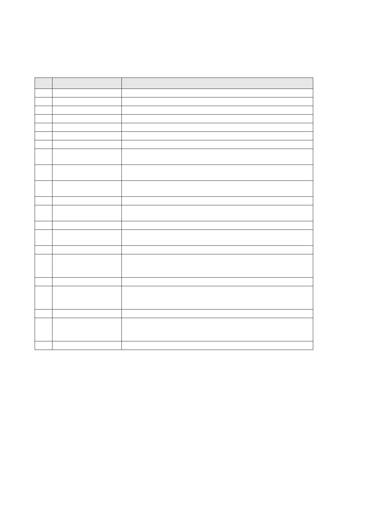
16.2.2 Pinout
The following table lists the JTAG+Trace connector pinout. It is compatible to the
"Trace Port Physical Interface" described in [ETM], 8.2.2 "Single target connector
pinout".
PIN SIGNAL Description
1 NC Not connected.
2 NC Not connected.
3 NC Not connected.
4 NC Not connected.
5 GND Signal ground.
6 TRACECLK Clocks trace data on rising edge or both edges.
7 DBGRQ Debug request.
8DBGACK
Debug acknowledge from the test chip, high when in
debug state.
9 RESET
Open-collector output from the run control to the target
system reset.
10 EXTTRIG
Optional external trigger signal to the Embedded trace
Macrocell (ETM). Not used. Leave open on target system.
11 TDO Test data output from target JTAG port.
12 VTRef
Signal level reference. It is normally fed from Vdd of the
target board and must not have a series resistor.
13 RTCK Return test clock from the target JTAG port.
14 VSupply
Supply voltage. It is normally fed from Vdd of the target
board and must not have a series resistor.
15 TCK Test clock to the run control unit from the JTAG port.
16 Trace signal 12
Trace signal. For more information, please refer to
Assignment of trace information pins between ETM archi-
tecture versions
on page 428.
17 TMS Test mode select from run control to the JTAG port.
18 Trace signal 11
Trace signal. For more information, please refer to
Assignment of trace information pins between ETM archi-
tecture versions
on page 428.
19 TDI Test data input from run control to the JTAG port.
20 Trace signal 10
Trace signal. For more information, please refer to
Assignment of trace information pins between ETM archi-
tecture versions
on page 428.
21 nTRST Active-low JTAG reset.
Table 16.7: JTAG+Trace connector pinout