40 CHAPTER 1 Introduction
J-Link / J-Trace (UM08001) ©
2004-2017 SEGGER Microcontroller GmbH & Co. KG
1.3.6.1 Additional features
• Very small form factor
• Fully software compatible to J-Link
• Supports any ARM7/9/11, Cortex-A5/A8/A9, Cortex-M0/M0+/M1/M3/M4, Cortex-
R4/R5 core
•JTAG clock up to 4 MHz
• SWD, SWO supported for Cortex-M devices
• Flash download into supported MCUs
• Standard 20-pin 0.1 inch JTAG connector (compatible to J-Link)
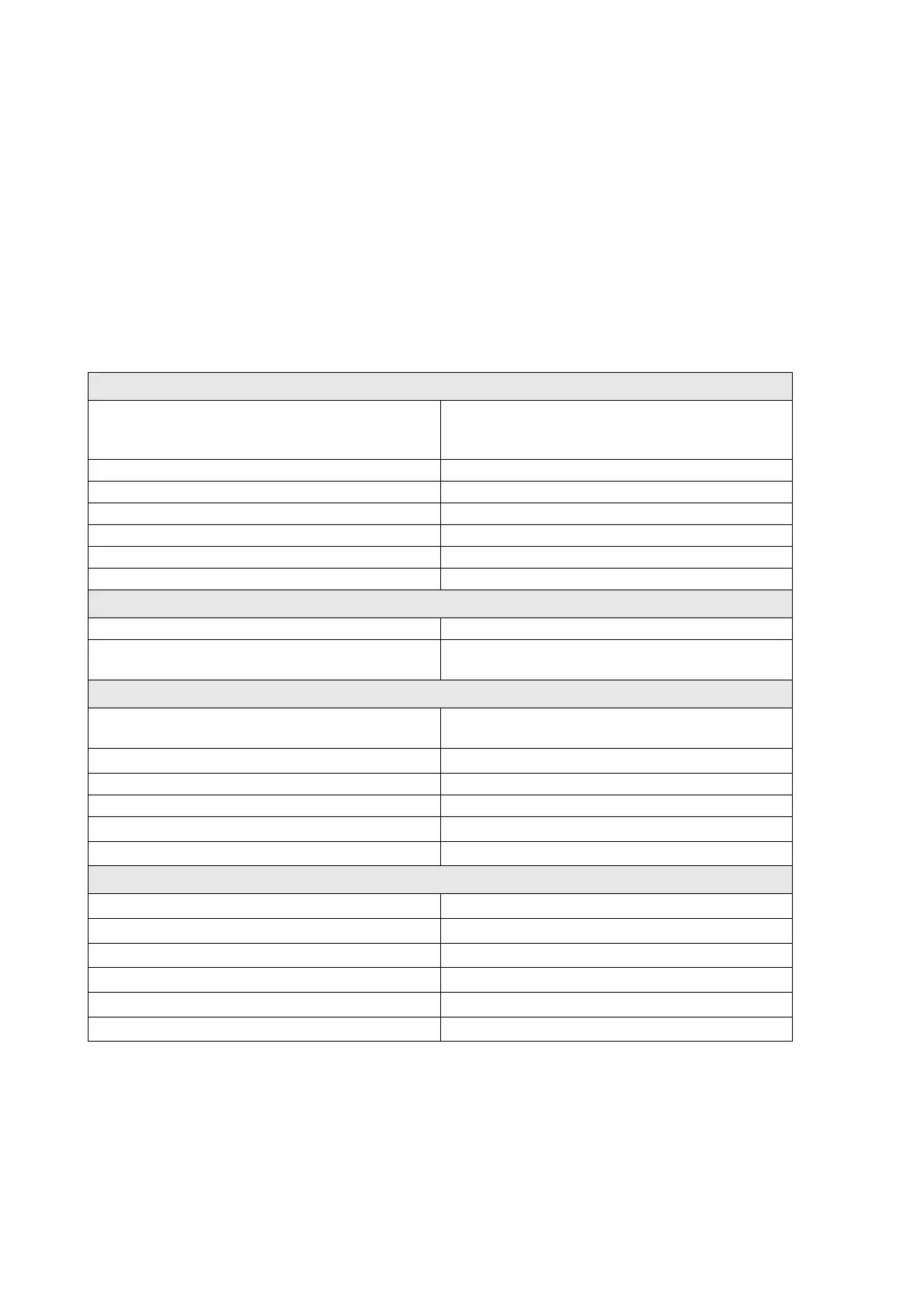
1.3.6.2 Specifications
The following table gives an overview about the specifications (general, mechanical,
electrical) for J-Link Lite ARM. All values are valid for J-Link hardware version 8.
1.3.6.3 Software and Hardware Features Overview
For detailed information about hardware and software features of your J-Link/J-Trace
model and version see:
https://wiki.segger.com/Software_and_Hardware_Features_Overview
General
Supported OS
For a complete list of all operating sys-
tems which are supported, please refer
to Supported OS on page 29.
Electromagnetic compatibility (EMC) EN 55022, EN 55024
Operating temperature +5°C ... +60°C
Storage temperature -20°C ... +65 °C
Relative humidity (non-condensing) Max. 90% rH
Size (without cables) 28mm x 26mm x 7mm
Weight (without cables) 6g
Mechanical
USB interface USB 2.0, full speed
Target interface
JTAG 20-pin
(14-pin adapter available)
JTAG/SWD Interface, Electrical
Power supply
USB powered
Max. 50mA + Target Supply current.
Target interface voltage (V
IF
)
3.3V
Target supply voltage 4.5V ... 5V (if powered with 5V on USB)
Target supply current Max. 300mA
LOW level input voltage (V
IL
) Max. 40% of V
IF
HIGH level input voltage (V
IH
) Min. 60% of V
IF
JTAG/SWD Interface, Timing
Data input rise time (T
rdi
)
Max. 20ns
Data input fall time (T
fdi
)
Max. 20ns
Data output rise time (T
rdo
)
Max. 10ns
Data output fall time (T
fdo
)
Max. 10ns
Clock rise time (T
rc
)
Max. 10ns
Clock fall time (T
fc
)
Max. 10ns
Table 1.4: J-Link Lite specifications