www.ti.com
Register Bit Definitions
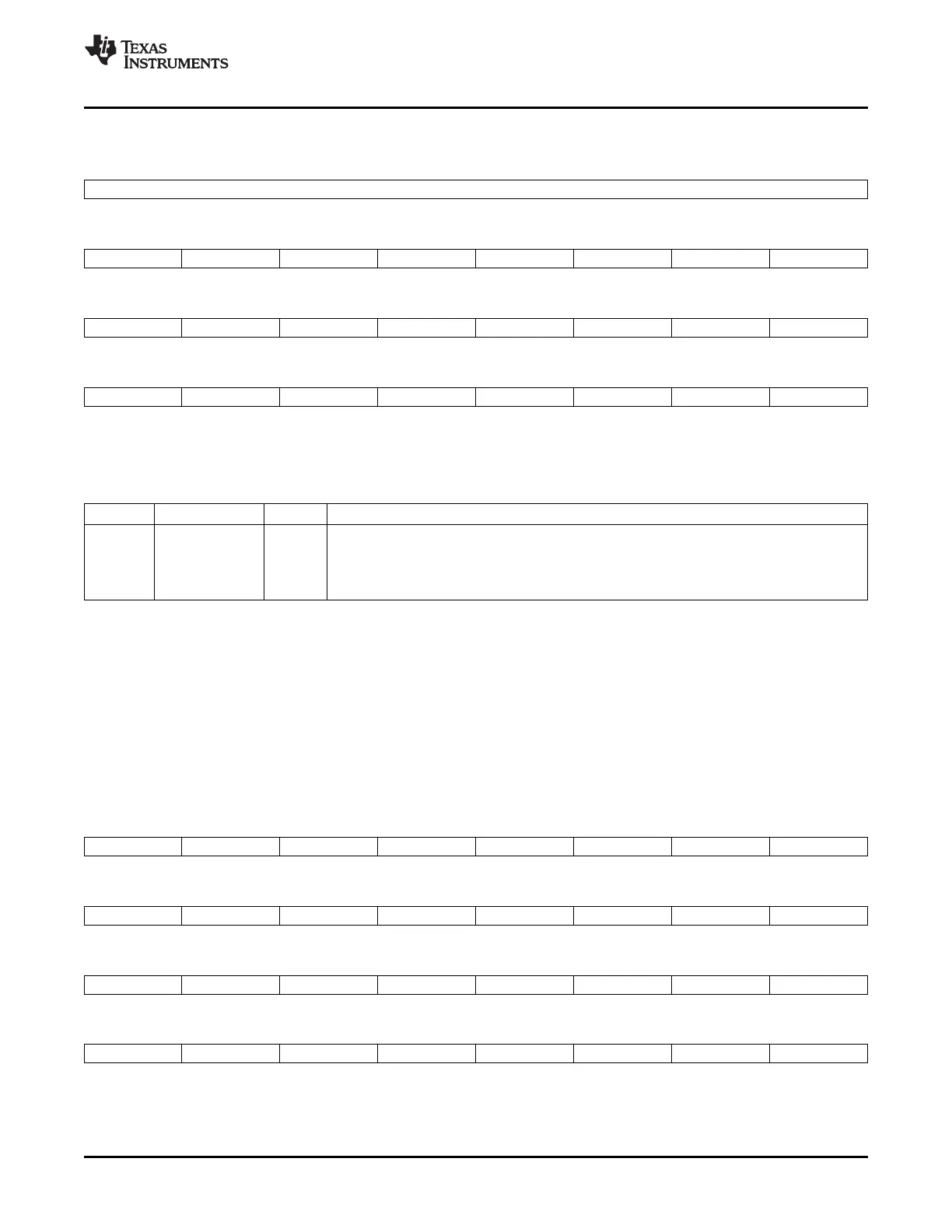
Figure 4-25. GPIO Port C Pullup Disable (GPCPUD) Registers
31 24
Reserved
R/W-0
23 22 21 20 19 18 17 16
GPIO87 GPIO86 GPIO85 GPIO84 GPIO83 GPIO82 GPIO81 GPIO80
R/W-0 R/W-0 R/W-0 R/W-0 R/W-0 R/W-0 R/W-0 R/W-0
15 14 13 12 11 10 9 8
GPIO79 GPIO78 GPIO77 GPIO76 GPIO75 GPIO74 GPIO73 GPIO72
R/W-0 R/W-0 R/W-0 R/W-0 R/W-0 R/W-0 R/W-0 R/W-0
7 6 5 4 3 2 1 0
GPIO71 GPIO70 GPIO69 GPIO68 GPIO67 GPIO66 GPIO65 GPIO64
R/W-0 R/W-0 R/W-0 R/W-0 R/W-0 R/W-0 R/W-0 R/W-0
LEGEND: R/W = Read/Write; R = Read only; - n = value after reset
Table 4-29. GPIO Port C Internal Pullup Disable (GPCPUD) Register Field Descriptions
Bits Field Value Description
(1)
31-0 GPIO87-GPIO64 Configure the internal pullup resister on the selected GPIO Port C pin. Each GPIO pin
corresponds to one bit in this register.
0 Enable the internal pullup on the specified pin.
1 Disable the internal pullup on the specified pin.
(1)
This register is EALLOW protected. See Section 5.2 for more information.
The GPIO data registers indicate the current status of the GPIO pin, irrespective of which mode the pin is
in. Writing to this register will set the respective GPIO pin high or low if the pin is enabled as a GPIO
output, otherwise the value written is latched but ignored. The state of the output register latch will remain
in its current state until the next write operation. A reset will clear all bits and latched values to zero. The
value read from the GPxDAT registers reflect the state of the pin (after qualification), not the state of the
output latch of the GPxDAT register.
Typically the DAT registers are used for reading the current state of the pins. To easily modify the output
level of the pin refer to the SET, CLEAR and TOGGLE registers.
Figure 4-26. GPIO Port A Data (GPADAT) Register
31 30 29 28 27 26 25 24
GPIO31 GPIO30 GPIO29 GPIO28 GPIO27 GPIO26 GPIO25 GPIO24
R/W-x R/W-x R/W-x R/W-x R/W-x R/W-x R/W-x R/W-x
23 22 21 20 19 18 17 16
GPIO23 GPIO22 GPIO21 GPIO20 GPIO19 GPIO18 GPIO17 GPIO16
R/W-x R/W-x R/W-x R/W-x R/W-x R/W-x R/W-x R/W-x
15 14 13 12 11 10 9 8
GPIO15 GPIO14 GPIO13 GPIO12 GPIO11 GPIO10 GPIO9 GPIO8
R/W-x R/W-x R/W-x R/W-x R/W-x R/W-x R/W-x R/W-x
7 6 5 4 3 2 1 0
GPIO7 GPIO6 GPIO5 GPIO4 GPIO3 GPIO2 GPIO1 GPIO0
R/W-x R/W-x R/W-x R/W-x R/W-x R/W-x R/W-x R/W-x
LEGEND: R/W = Read/Write; R = Read only; - n = value after reset
(1)
(1)
x = The state of the GPADAT register is unknown after reset. It depends on the level of the pin after reset.
SPRUFB0C – September 2007 – Revised May 2009 General-Purpose Input/Output (GPIO) 101
Submit Documentation Feedback
 Loading...