Register Bit Definitions
www.ti.com
Table 4-16. GPIO Port C MUX 1 (GPCMUX1) Register Field Descriptions (continued)
Bit Field Value Description
15:14 GPIO71 Configure this pin as:
00 or 01 GPIO 71 - general purpose I/O 71 (default)
10 or 11 XD8 - External interface data line 8 (O)
13:12 GPIO70 Configure this pin as:
00 or 01 GPIO 70 - general purpose I/O 70 (default)
10 or 11 XD9 - External interface data line 9 (O)
11:10 GPIO69 Configure this pin as:
00 or 01 GPIO 69 - general purpose I/O 69 (default)
10 or 11 XD10 - External interface data line 10 (O)
9:8 GPIO68 Configure this pin as:
00 or 01 GPIO 68 - general purpose I/O 68 (default)
10 or 11 XD11 - External interface data line 11 (O)
7:6 GPIO67 Configure this pin as:
00 or 01 GPIO 67 - general purpose I/O 67 (default)
10 or 11 XD12 - External interface data line 12 (O)
5:4 GPIO66 Configure this pin as:
00 or 01 GPIO 66 - general purpose I/O 66 (default)
10 or 11 XD13 - External interface data line 13 (O)
3:2 GPIO65 Configure this pin as:
00 or 01 GPIO 65 - general purpose I/O 65 (default)
10 or 11 XD14 - External interface data line 14 (O)
1:0 GPIO64 Configure this pin as:
00 or 01 GPIO 64 - general purpose I/O 64 (default)
10 or 11 XD15 - External interface data line 15 (O)
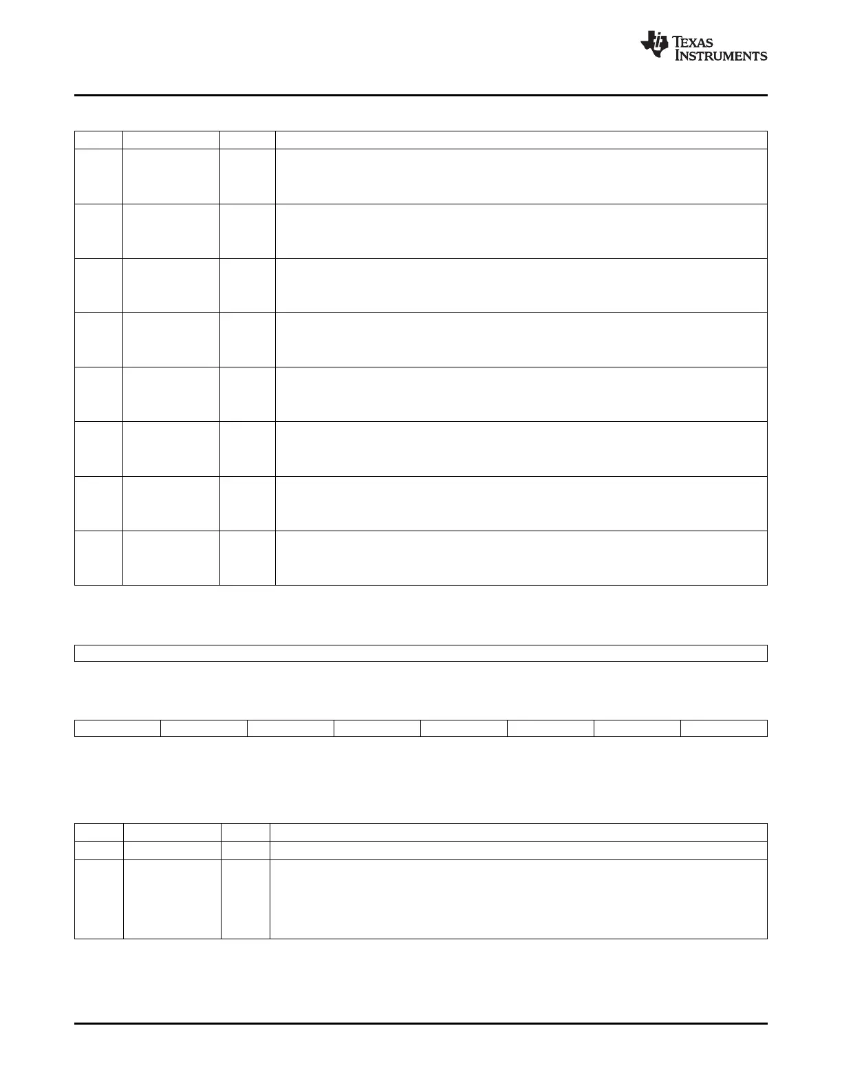
Figure 4-13. GPIO Port C MUX 2 (GPCMUX2) Register
31 16
Reserved
R-0
15 14 13 12 11 10 9 8 7 6 5 4 3 2 1 0
GPIO87 GPIO86 GPIO85 GPIO84 GPIO83 GPIO82 GPIO81 GPIO80
R/W-0 R/W-0 R/W-0 R/W-0 R/W-0 R/W-0 R/W-0 R/W-0
LEGEND: R/W = Read/Write; R = Read only; - n = value after reset
Table 4-17. GPIO Port C MUX 2 (GPCMUX2) Register Field Descriptions
Bit Field Value Description
31:16 Reserved
15:14 GPIO87 Configure this pin as:
00 or GPIO 87 - general purpose I/O 87 (default)
01
10 or XA15 - External interface address line 15 (O)
11
92 General-Purpose Input/Output (GPIO) SPRUFB0C – September 2007 – Revised May 2009
Submit Documentation Feedback
 Loading...