www.ti.com
Clocking and System Control
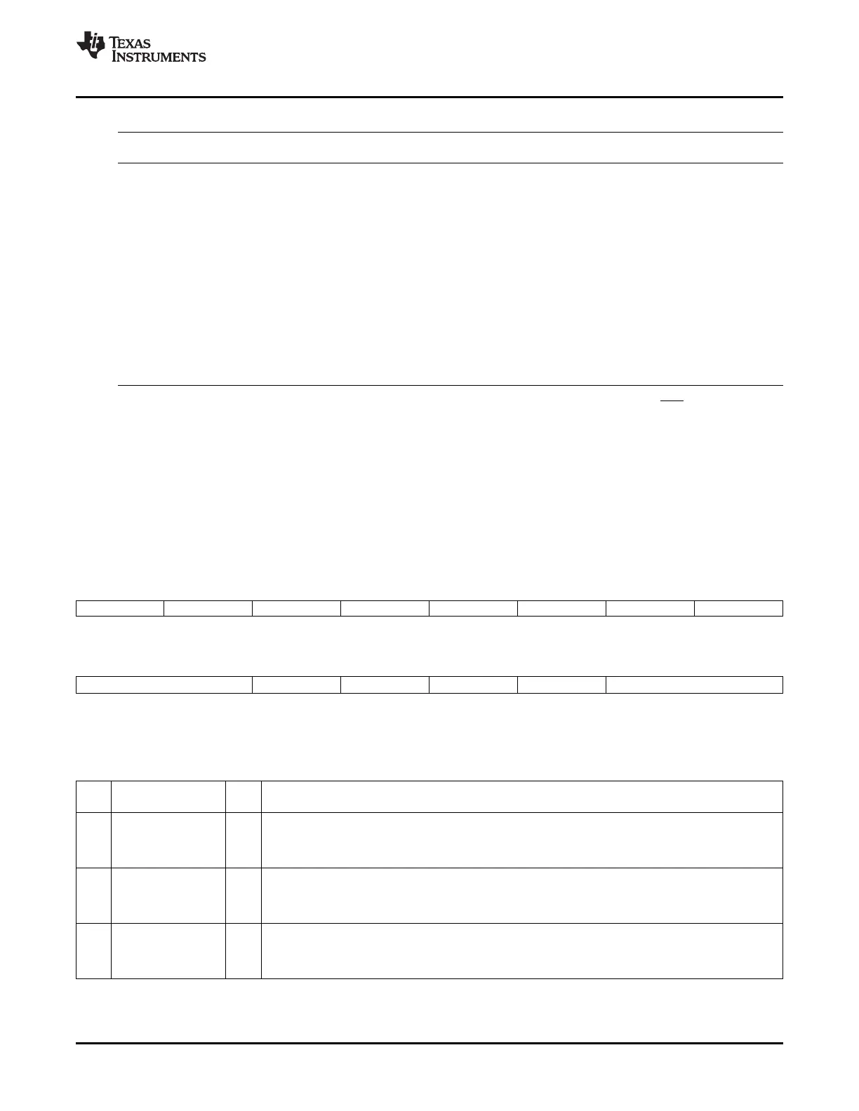
Table 3-1. PLL, Clocking, Watchdog, and Low-Power Mode Registers
Name Address Size Description
(1)
Bit Description
(x16)
PLLSTS
(2)
0x7011 1 PLL Status Register Figure 3-12
HISPCP 0x701A 1 High-Speed Peripheral Clock (HSPCLK) Prescaler Register Figure 3-5
LOSPCP 0x701B 1 Low-Speed Peripheral Clock (LSPCLK) Prescaler Register Figure 3-6
PCLKCR0 0x701C 1 Peripheral Clock Control Register 0 Figure 3-2
PCLKCR1 0x701D 1 Peripheral Clock Control Register 1 Figure 3-3
LPMCR0 0x701E 1 Low Power Mode Control Register 0 Figure 3-6
PCLKCR3 0x7020 1 Peripheral Clock Control Register 3 Figure 3-4
PLLCR
(2)
0x7021 1 PLL Control Register Figure 3-11
SCSR 0x7022 1 System Control & Status Register Figure 3-15
WDCNTR 0x7023 1 Watchdog Counter Register. Figure 3-16
WDKEY 0x7025 1 Watchdog Reset Key Register Figure 3-17
WDCR 0x7029 1 Watchdog Control Register Figure 3-18
(1)
All of the registers in this table are EALLOW protected. See Section 5.2 for more information.
(2)
The PLL control register (PLLCR) and PLL Status Register (PLLSTS) are reset to a known state by the XRS signal or a
watchdog reset only. A reset issued by the debugger or the missing clock detect logic have no effect.
The PCLKCR0 /1/3 registers enable/disable clocks to the various peripheral modules. There is a
2-SYSCLKOUT cycle delay from when a write to the PCLKCR0 /1/3 registers occurs to when the action is
valid. This delay must be taken into account before attempting to access the peripheral configuration
registers. Due to the peripheral-GPIO MUXing, all peripherals cannot be used at the same time. While it is
possible to turn on the clocks to all the peripherals at the same time, such a configuration is not useful. If
this is done, the current drawn will be more than required. To avoid this, only enable the clocks required
by the application.
Figure 3-2. Peripheral Clock Control 0 Register (PCLKCR0)
15 14 13 12 11 10 9 8
ECANBENCLK ECANAENCLK MCBSPBENCLK MCBSPAENCLK SCIBENCLK SCIAENCLK Reserved SPIAENCLK
R/W-0 R/W-0 R/W-0 R/W-0 R/W-0 R/W-0 R-0 R/W-0
7 6 5 4 3 2 1 0
Reserved SCICENCLK I2CAENCLK ADCENCLK TBCLKSYNC Reserved
R-0 R/W-0 R/W-0 R/W-0 R/W-0 R-0
LEGEND: R/W = Read/Write; R = Read only; - n = value after reset
Table 3-2. Peripheral Clock Control 0 Register (PCLKCR0) Field Descriptions
Bit Field Valu Description
(1)
e
15 ECANBENCLK ECAN-B Clock enable
0 The eCAN-B module is not clocked. (default)
(2)
1 The eCAN-B module is clocked (SYSCLKOUT/2).
14 ECANAENCLK ECAN-A clock enable
0 The eCAN-A module is not clocked. (default)
(2)
1 The eCAN-A module is clocked (SYSCLKOUT/2).
13 MCBSPBENCLK McBSP-B Clock Enable. This bit is reserved on devices without the McBSP-B module.
(3)
0 The McBSP-B module is not clocked. (default)
1 The McBSP-B module is clocked by the low-speed clock (LSPCLK).
(1)
This register is EALLOW protected. See Section 5.2 for more information.
(2)
If a peripheral block is not used, the clock to that peripheral can be turned off to minimize power consumption.
(3)
On devices without a particular peripheral, the clock selection bit is reserved. On these devices, the bit should not be written to with a 1.
SPRUFB0C – September 2007 – Revised May 2009 Clocking 39
Submit Documentation Feedback
 Loading...