www.ti.com
Register Bit Definitions
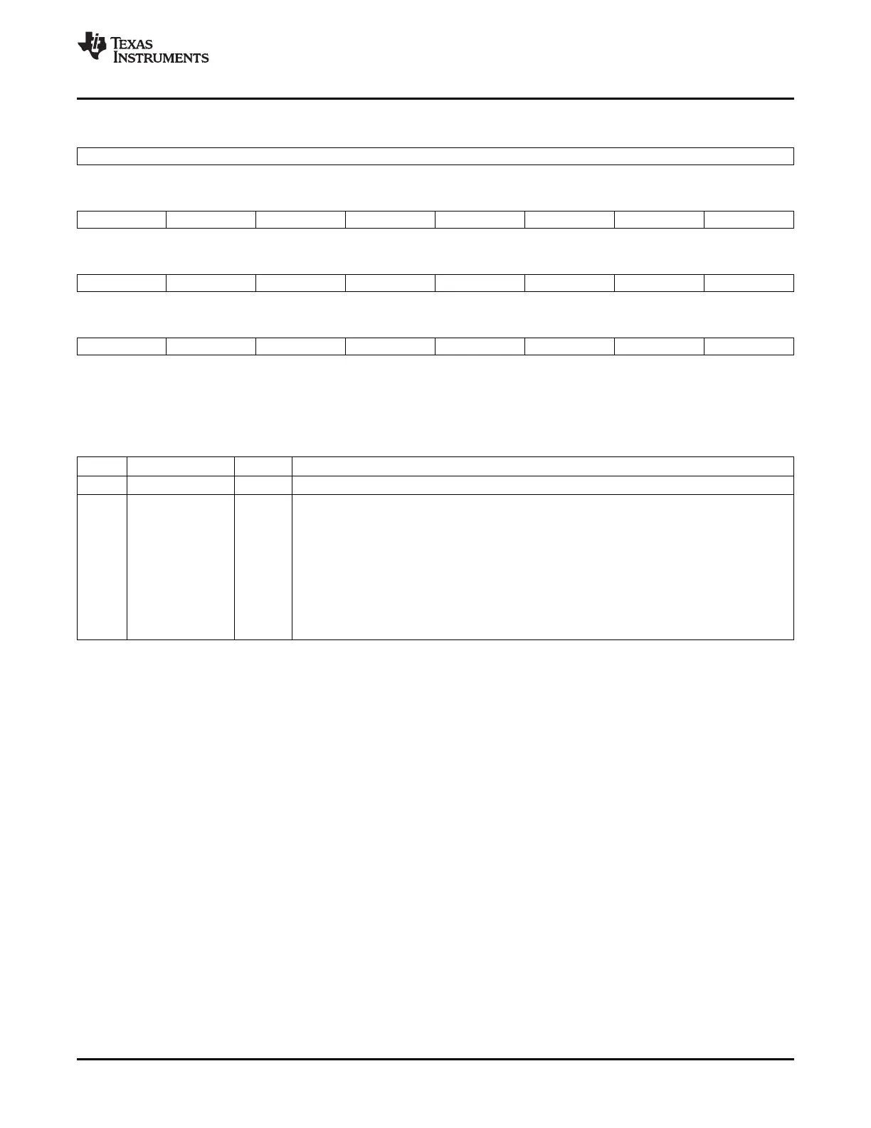
Figure 4-28. GPIO Port C Data (GPCDAT) Register
31 24
Reserved
R-0
23 22 21 20 19 18 17 16
GPIO87 GPIO86 GPIO85 GPIO84 GPIO83 GPIO82 GPIO81 GPIO80
R/W-x R/W-x R/W-x R/W-x R/W-x R/W-x R/W-x R/W-x
15 14 13 12 11 10 9 8
GPIO79 GPIO78 GPIO77 GPIO76 GPIO75 GPIO74 GPIO73 GPIO72
R/W-x R/W-x R/W-x R/W-x R/W-x R/W-x R/W-x R/W-x
7 6 5 4 3 2 1 0
GPIO71 GPIO70 GPIO69 GPIO68 GPIO67 GPIO66 GPIO65 GPIO64
R/W-x R/W-x R/W-x R/W-x R/W-x R/W-x R/W-x R/W-x
LEGEND: R/W = Read/Write; R = Read only; - n = value after reset
(1)
(1)
x = The state of the GPADAT register is unknown after reset. It depends on the level of the pin after reset.
Table 4-32. GPIO Port C Data (GPCDAT) Register Field Descriptions
Bit Field Value Description
31-3 Reserved Reserved
2-0 GPIO87-GPIO64 Each bit corresponds to one GPIO port B pin (GPIO64-GPIO87) as shown in Figure 4-28
0 Reading a 0 indicates that the state of the pin is currently low, irrespective of the mode the pin is
configured for.
Writing a 0 will force an output of 0 if the pin is configured as a GPIO output in the appropriate
GPCMUX1 and GPCDIR registers; otherwise, the value is latched but not used to drive the pin.
1 Reading a 1 indicates that the state of the pin is currently high irrespective of the mode the pin is
configured for.
Writing a 1 will force an output of 1 if the pin is configured as a GPIO output in the GPCMUX1
and GPCDIR registers; otherwise, the value is latched but not used to drive the pin.
SPRUFB0C – September 2007 – Revised May 2009 General-Purpose Input/Output (GPIO) 103
Submit Documentation Feedback
 Loading...