6.3.3 Flow of a Multiplexed Interrupt Request From a Peripheral to the CPU
Peripheral
IE/IF
PIEIFRx.1
latch
PIE
interrupt
flag
PIEIERx.1
Highest
Vector
0
1
0
1
PIEIFRx.8
Vector
latch
Peripheral
IE/IF
1
0
1
0
Lowest
PIEIERx.8
8 interrupts
per group
Search order
highest to
lowest
Pulse
gen
PIEACKx
0
1
1
2
3a
interrupt
enable
PIE
3b
4
Vector is fetched
only after CPU
interrupt logic
has recognized
the interrupt
9
IFRx
latch
1=valid Int
IERx
1
0
5
6
1
0
INTM
7
CPU
interrupt
logic
8
CPU
PIE group
acknowledge
www.ti.com
Interrupt Sources
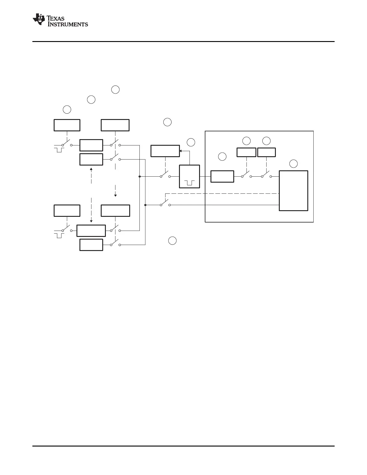
Figure 6-6 shows the flow with the steps shown in circled numbers. Following the diagram, the steps are
described.
Figure 6-6. Multiplexed Interrupt Request Flow Diagram
Step 1. Any peripheral or external interrupt within the PIE group generates an interrupt. If interrupts
are enabled within the peripheral module then the interrupt request is sent to the PIE module.
Step 2. The PIE module recognizes that interrupt y within PIE group x (INTx.y) has asserted an
interrupt and the appropriate PIE interrupt flag bit is latched: PIEIFRx.y = 1.
Step 3. For the interrupt request to be sent from the PIE to the CPU, both of the following conditions
must be true:
a. The proper enable bit must be set (PIEIERx.y = 1) and
b. The PIEACKx bit for the group must be clear.
Step 4. If both conditions in 3a and 3b are true, then an interrupt request is sent to the CPU and the
acknowledge bit is again set (PIEACKx = 1). The PIEACKx bit will remain set until you clear it
to indicate that additional interrupts from the group can be sent from the PIE to the CPU.
Step 5. The CPU interrupt flag bit is set (CPU IFRx = 1) to indicate a pending interrupt x at the CPU
level.
Step 6. If the CPU interrupt is enabled (CPU IER bit x = 1, or DBGIER bit x = 1) AND the global
interrupt mask is clear (INTM = 0) then the CPU will service the INTx.
Step 7. The CPU recognizes the interrupt and performs the automatic context save, clears the IER
bit, sets INTM, and clears EALLOW. All of the steps that the CPU takes in order to prepare to
service the interrupt are documented in the TM S320C28x DSP CPU and Instruction Set
Reference Guide (literature number SPRU430).
Step 8. The CPU will then request the appropriate vector from the PIE.
Step 9. For multiplexed interrupts, the PIE module uses the current value in the PIEIERx and
PIEIFRx registers to decode which vector address should be used. There are two possible
cases:
SPRUFB0C – September 2007 – Revised May 2009 Peripheral Interrupt Expansion (PIE) 131
Submit Documentation Feedback
 Loading...