4.1 GPIO Module Overview
GPADAT
(latch)
GPACLEAR,
GPATOGGLE
GPAQSEL 1/2
Qual
GPAMUX 1/2
SYSCLKOUT
High
impedance
output
control
GPIO0
to
GPIO27
Pins
PU
XRS
Sync
Lowpower
modesblock
GPIOx.async
GPADIR
(latch)
01
11
01
GPACTRL
2
2
10
Peripheral1input
N/C
(defaultonreset)
(defaultonreset)
GPIOx_OUT
GPIOx_DIR
GPAPUD
0 = enablePU
1 = disablePU
(disabledafterreset)
async
(asyncdisable
whenlow)
11
10
Peripheral2input
Peripheral3input
Peripheral1output
GPASET,
(default
onreset)
3samples
6samples
00
00
XRS
(defaultonreset)
01
11
10
00
01
11
10
00
0=input,1=output
GPIOXINT1SEL
GPIOXINT2SEL
GPIOXNMISEL
External
interrupt
MUX
PIE
GPADAT (read)
GPIOLPMSEL
LPMCR0
Peripheral2output
Peripheral3output
Peripheral1outputenable
Peripheral2outputenable
Peripheral3outputenable
GPIO Module Overview
www.ti.com
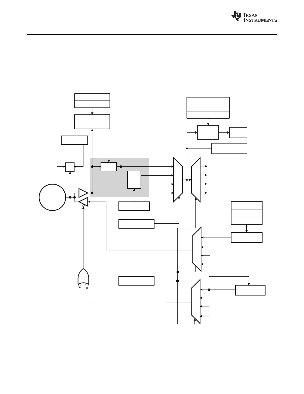
Up to three independent peripheral signals are multiplexed on a single GPIO-enabled pin in addition to
individual pin bit-I/O capability. There are three 32-bit I/O ports. Port A consists of GPIO0-GPIO31, port B
consists of GPIO32-GPIO63, and port C consists of GPIO64-87. Figure 4-1 shows the basic modes of
operation for the GPIO module.
Figure 4-1. GPIO0 to GPIO27 Multiplexing Diagram
A GPxDAT latch/read are accessed at the same memory location.
66 General-Purpose Input/Output (GPIO) SPRUFB0C – September 2007 – Revised May 2009
Submit Documentation Feedback
 Loading...