www.ti.com
Clocking and System Control
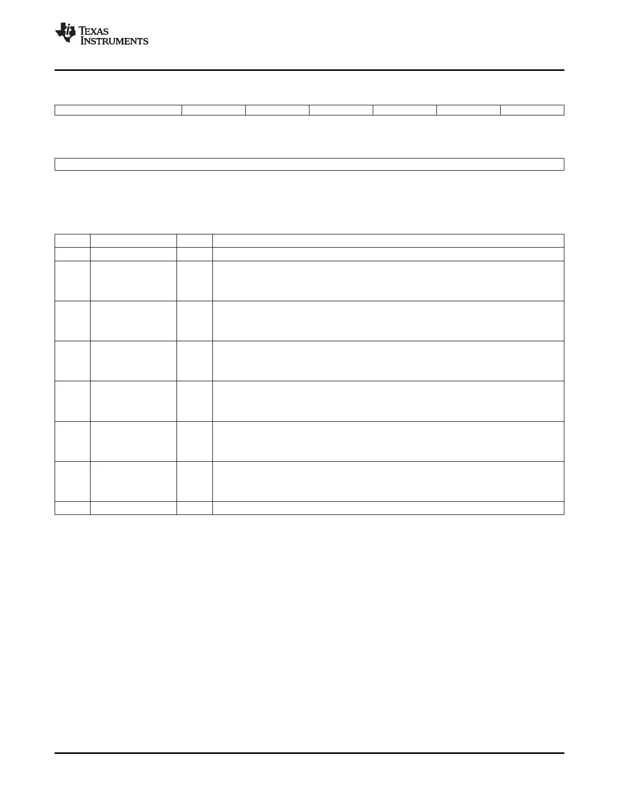
Figure 3-4. Peripheral Clock Control 3 Register (PCLKCR3)
15 14 13 12 11 10 9 8
Reserved GPIOINENCLK XINTFENCLK DMAENCLK CPUTIMER2ENCLK CPUTIMER1ENCLK CPUTIMER0ENCLK
R-0 R/W-1 R/W-0 R/W-0 R/W-1 R/W-1 R/W-1
7 0
Reserved
R-0
LEGEND: R/W = Read/Write; R = Read only; - n = value after reset
Table 3-4. Peripheral Clock Control 3 Register (PCLKCR3) Field Descriptions
Bit Field Value Description
15:`14 Reserved Reserved
13 GPIOINENCLK GPIO Input Clock Enable
0 The GPIO module is not clocked.
1 The GPIO module is clocked.
12 XINTFENCLK External Interface (XINTF) Clock Enable
0 The external memory interface is not clocked.
1 The external memory interface is clocked.
11 DMAENCLK DMA Clock Enable
0 The DMA module is not clocked.
1 The DMA module is clocked.
10 CPUTIMER2ENCLK CPU Timer 2 Clock Enable
0 The CPU Timer 2 is not clocked.
1 The CPU Timer 2 is clocked.
9 CPUTIMER1ENCLK CPU Timer 1 Clock Enable
0 The CPU Timer 1 is not clocked.
1 The CPU Timer 1 is clocked.
8 CPUTIMER0ENCLK CPU Timer 0 Clock Enable
0 The CPU Timer 0 is not clocked.
1 The CPU Timer 0 is clocked.
7:0 Reserved Reserved
The high speed peripheral and low speed peripheral clock prescale (HISPCP and LOSPCP) registers are
used to configure the high- and low-speed peripheral clocks, respectively. See Figure 3-5 for the HISPCP
bit layout and Figure 3-6 for the LOSPCP layout.
SPRUFB0C – September 2007 – Revised May 2009 Clocking 43
Submit Documentation Feedback
 Loading...