Register Bit Definitions
www.ti.com
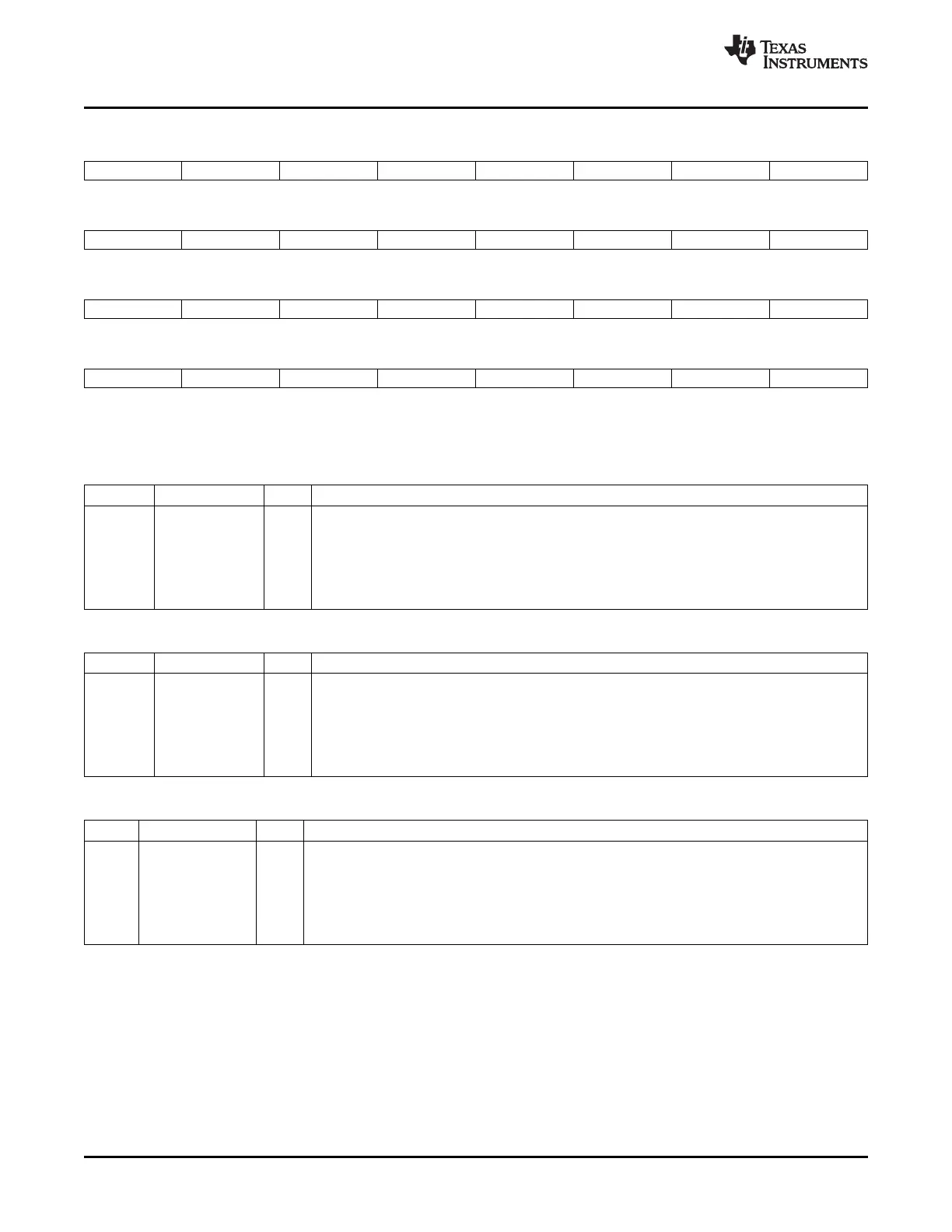
Figure 4-29. GPIO Port A Set, Clear and Toggle (GPASET, GPACLEAR, GPATOGGLE) Registers
31 30 29 28 27 26 25 24
GPIO31 GPIO30 GPIO29 GPIO28 GPIO27 GPIO26 GPIO25 GPIO24
R/W-0 R/W-0 R/W-0 R/W-0 R/W-0 R/W-0 R/W-0 R/W-0
23 22 21 20 19 18 17 16
GPIO23 GPIO22 GPIO21 GPIO20 GPIO19 GPIO18 GPIO17 GPIO16
R/W-0 R/W-0 R/W-0 R/W-0 R/W-0 R/W-0 R/W-0 R/W-0
15 14 13 12 11 10 9 8
GPIO15 GPIO14 GPIO13 GPIO12 GPIO11 GPIO10 GPIO9 GPIO8
R/W-0 R/W-0 R/W-0 R/W-0 R/W-0 R/W-0 R/W-0 R/W-0
7 6 5 4 3 2 1 0
GPIO7 GPIO6 GPIO5 GPIO4 GPIO3 GPIO2 GPIO1 GPIO0
R/W-0 R/W-0 R/W-0 R/W-0 R/W-0 R/W-0 R/W-0 R/W-0
LEGEND: R/W = Read/Write; R = Read only; - n = value after reset
Table 4-33. GPIO Port A Set (GPASET) Register Field Descriptions
Bits Field Value Description
31-0 GPIO31-GPIO0 Each GPIO port A pin (GPIO0-GPIO31) corresponds to one bit in this register as shown in
Figure 4-29 .
0 Writes of 0 are ignored. This register always reads back a 0.
1 Writing a 1 forces the respective output data latch to high. If the pin is configured as a GPIO
output then it will be driven high. If the pin is not configured as a GPIO output then the latch is set
high but the pin is not driven.
Table 4-34. GPIO Port A Clear (GPACLEAR) Register Field Descriptions
Bits Field Value Description
31-0 GPIO31 - GPIO0 Each GPIO port A pin (GPIO0-GPIO31) corresponds to one bit in this register as shown in
Figure 4-29 .
0 Writes of 0 are ignored. This register always reads back a 0.
1 Writing a 1 forces the respective output data latch to low. If the pin is configured as a GPIO output
then it will be driven low. If the pin is not configured as a GPIO output then the latch is cleared but
the pin is not driven.
Table 4-35. GPIO Port A Toggle (GPATOGGLE) Register Field Descriptions
Bits Field Value Description
31-0 GPIO31-GPIO0 Each GPIO port A pin (GPIO0-GPIO31) corresponds to one bit in this register as shown in
Figure 4-29 .
0 Writes of 0 are ignored. This register always reads back a 0.
1 Writing a 1 forces the respective output data latch to toggle from its current state. If the pin is
configured as a GPIO output then it will be driven in the opposite direction of its current state. If the
pin is not configured as a GPIO output then the latch is toggled but the pin is not driven.
General-Purpose Input/Output (GPIO)104 SPRUFB0C – September 2007 – Revised May 2009
Submit Documentation Feedback
 Loading...