Flash and OTP Registers
www.ti.com
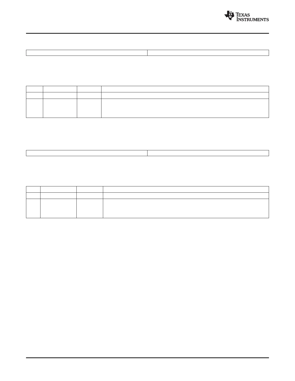
Figure 1-7. Flash Standby Wait Register (FSTDBYWAIT)
15 9 8 0
Reserved STDBYWAIT
R-0 R/W-1
LEGEND: R/W = Read/Write; R = Read only; - n = value after reset
Table 1-5. Flash Standby Wait Register (FSTDBYWAIT) Field Descriptions
Bit Field Value Description
(1) (2)
15-9 Reserved 0 Reserved
8-0 STDBYWAIT This register should be left in its default state.
Bank and Pump Sleep To Standby Wait Count.
111111111 511 SYSCLKOUT cycles (default)
(1)
This register is EALLOW protected. See Section 5.2 for more information.
(2)
This register is protected by the Code Security Module (CSM). See Chapter 2 for more information.
Figure 1-8. Flash Standby to Active Wait Counter Register (FACTIVEWAIT)
7 9 8 0
Reserved ACTIVEWAIT
R-0 R/W-1
LEGEND: R/W = Read/Write; R = Read only; - n = value after reset
Table 1-6. Flash Standby to Active Wait Counter Register (FACTIVEWAIT) Field Descriptions
Bits Field Value Description
(1) (2)
15-9 Reserved 0 Reserved
8-0 ACTIVEWAIT This register should be left in its default state.
Bank and Pump Standby To Active Wait Count:
111111111 511 SYSCLKOUT cycles (default)
(1)
This register is EALLOW protected. See Section 5.2 for more information.
(2)
This register is protected by the Code Security Module (CSM). See Chapter 2 for more information.
Flash and OTP Memory Blocks24 SPRUFB0C – September 2007 – Revised May 2009
Submit Documentation Feedback
 Loading...