www.ti.com
Register Bit Definitions
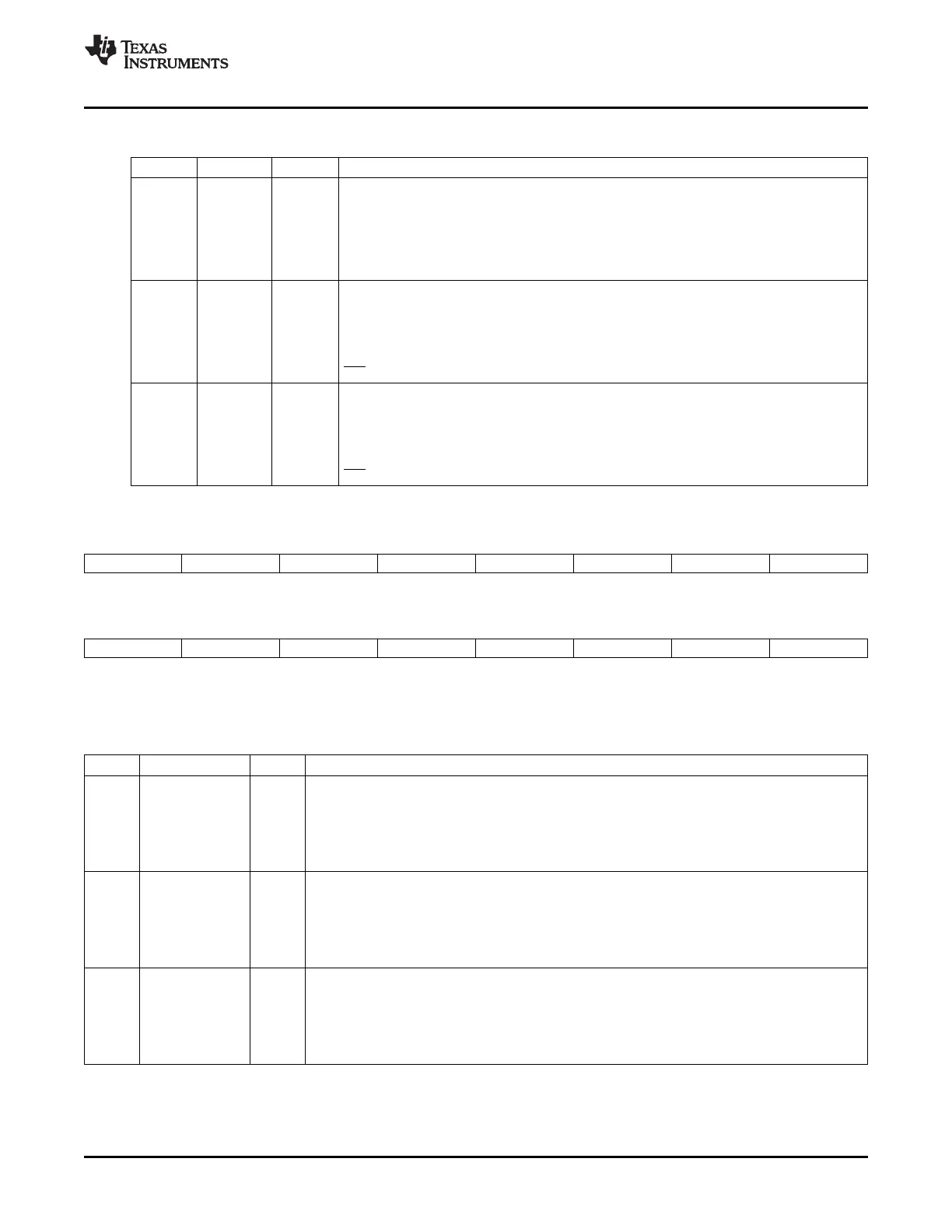
Table 4-13. GPIO Port A MUX 2 (GPAMUX2) Register Field Descriptions (continued)
Bits Field Value Description
(1)
5-4 GPIO18 Configure the GPIO18 pin as:
00 GPIO18 - General purpose I/O 18 (default) (I/O)
01 SPICLKA - SPI-A clock (I/O)
10 SCITXDB - SCI-B transmit. (O)
11 CANRXA - eCAN-A Receive (I)
3-2 GPIO17 Configure the GPIO17 pin as:
00 GPIO17 - General purpose I/O 17 (default) (I/O)
01 SPISOMIA - SPI-A slave-out, master-in (I/O)
10 CANRXB eCAN-B receive (I)
11 TZ6 - Trip zone 6 (I)
1-0 GPIO16 Configure the GPIO16 pin as:
00 GPIO16 - General purpose I/O 16 (default) (I/O)
01 SPISIMOA - SPI-A slave-in, master-out (I/O),
10 CANTXB - eCAN-B transmit. (O)
11 TZ5 - Trip zone 5 (I)
Figure 4-10. GPIO Port B MUX 1 (GPBMUX1) Register
31 30 29 28 27 26 25 24 23 22 21 20 19 18 17 16
GPIO47 GPIO46 GPIO45 GPIO44 GPIO43 GPIO42 GPIO41 GPIO40
R/W-0 R/W-0 R/W-0 R/W-0 R/W-0 R/W-0 R/W-0 R/W-0
15 14 13 12 11 10 9 8 7 6 5 4 3 2 1 0
GPIO39 GPIO38 GPIO37 GPIO36 GPIO35 GPIO34 GPIO33 GPIO32
R/W-0 R/W-0 R/W-0 R/W-0 R/W-0 R/W-0 R/W-0 R/W-0
LEGEND: R/W = Read/Write; R = Read only; - n = value after reset
Table 4-14. GPIO Port B MUX 1 (GPBMUX1) Register Field Descriptions
Bit Field Value Description
31:30 GPIO47 Configure this pin as:
00 GPIO 47 - general purpose I/O 47 (default)
01 Reserved
10 or XA7 - External interface (XINTF) address line 7 (O)
11
29:28 GPIO46 Configure this pin as:
00 GPIO 46 - general purpose I/O 46 (default)
01 Reserved
10 or XA6 - External interface (XINTF) address line 6 (O)
11
27:26 GPIO45 Configure this pin as:
00 GPIO 45 - general purpose I/O 45 (default)
01 Reserved
10 or XA5 - External interface (XINTF) address line 5 (O)
11
SPRUFB0C – September 2007 – Revised May 2009 General-Purpose Input/Output (GPIO) 87
Submit Documentation Feedback
 Loading...