www.ti.com
Register Bit Definitions
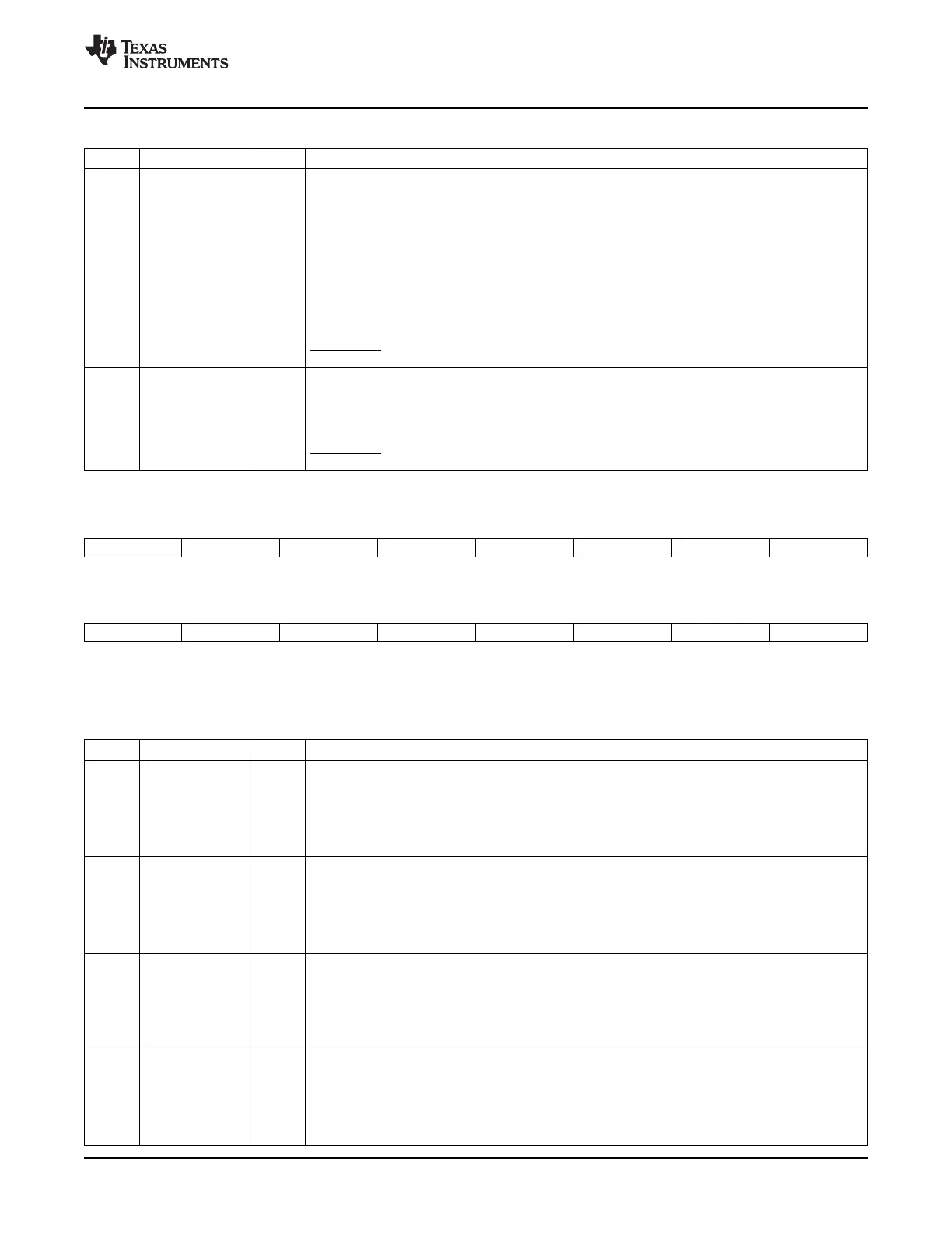
Table 4-14. GPIO Port B MUX 1 (GPBMUX1) Register Field Descriptions (continued)
Bit Field Value Description
5:4 GPIO34 Configure this pin as:
00 GPIO 34 - general purpose I/O 34 (default)
01 ECAPI - Enhanced capture input/output 1 (I/O)
10 or XREADY - External interface ready signal
11
3:2 GPIO33 Configure this pin as:
00 GPIO 33 - general purpose I/O 33 (default)
01 SCLA - I2C clock open drain bidirectional port (I/O)
10 EPWMSYNCO - External ePWM sync pulse output (O)
11 ADCSOCBO - ADC start-of-conversion B (O)
1:0 GPIO32 Configure this pin as:
00 GPIO 32 - general purpose I/O 32 (default)
01 SDAA - I2C data open drain bidirectional port (I/O)
10 EPWMSYNCI - External ePWM sync pulse input (I)
11 ADCSOCAO - ADC start-of-conversion A (O)
Figure 4-11. GPIO Port B MUX 2 (GPBMUX2) Register
31 30 29 28 27 26 25 24 23 22 21 20 19 18 17 16
GPIO63 GPIO62 GPIO61 GPIO60 GPIO59 GPIO58 GPIO57 GPIO56
R/W-0 R/W-0 R/W-0 R/W-0 R/W-0 R/W-0 R/W-0 R/W-0
15 14 13 12 11 10 9 8 7 6 5 4 3 2 1 0
GPIO55 GPIO54 GPIO53 GPIO52 GPIO51 GPIO50 GPIO49 GPIO48
R/W-0 R/W-0 R/W-0 R/W-0 R/W-0 R/W-0 R/W-0 R/W-0
LEGEND: R/W = Read/Write; R = Read only; - n = value after reset
Table 4-15. GPIO Port B MUX 2 (GPBMUX2) Register Field Descriptions
Bit Field Value Description
31:30 GPIO63 Configure this pin as:
00 GPIO 63 - general purpose I/O 63 (default)
01 GPIO 63 - general purpose I/O 63 (default)
10 or XD16 - External interface data line 16 (I/O)
11
29:28 GPIO62 Configure this pin as:
00 GPIO 62 - general purpose I/O 62 (default)
01 SCIRXDC - SCI-C receive data (I)
10 or XD17 - External interface data line 17 (I/O)
11
27:26 GPIO61 Configure this pin as:
00 GPIO 61 - general purpose I/O 61 (default)
01 MFSRB - McBSP-B receive frame synch (I/O)
10 or XD18 - External interface data line 18 (I/O)
11
25:24 GPIO60 Configure this pin as:
00 GPIO 60 - general purpose I/O 60 (default)
01 MCLKRB - McBSP-B receive clock (I/O)
10 or XD19 - External interface data line 19 (I/O)
11
SPRUFB0C – September 2007 – Revised May 2009 General-Purpose Input/Output (GPIO) 89
Submit Documentation Feedback
 Loading...