3.1 Clocking and System Control
ePWM1/../6,HRPWM1/../6,
eCAP1/../6,eQEP1/2
Peripheral
Registers
Bridge
ClockEnables
I/O
Peripheral
Registers
ClockEnables
I/O
eCAN-A/B
/2
Peripheral
Registers
ClockEnables
I/O
SPI-A,SCI-A/B/C
LOSPCP
LSPCLK
System
Control
Register
Bridge
SYSCLKOUT
MemoryBus
C28xCore
GPIO
Mux
ClockEnables
Peripheral
Registers
I/O
McBSP-A/B
LOSPCP
LSPCLK
ClockEnables
Bridge
HISPCP
HSPCLK
DMA
Bus
Result
Registers
Bridge
12-Bit ADC
ADC
Registers
16Channels
DMA
ClockEnables
PeripheralBus
CLKIN
I2C-A
ClockEnables
Clocking and System Control
www.ti.com
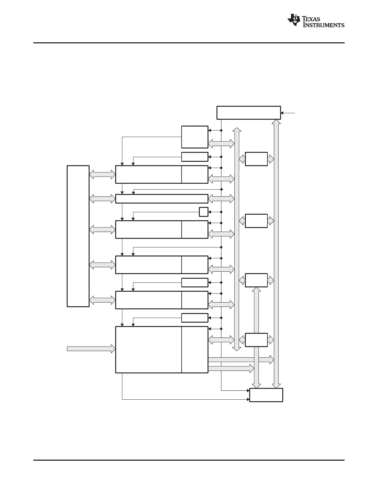
Figure 3-1 shows the various clock and reset domains.
The PLL, clocking, watchdog and low-power modes, are controlled by the registers listed in Table 3-1 .
Figure 3-1. Clock and Reset Domains
A CLKIN is the clock into the CPU. It is passed out of the CPU as SYSCLKOUT (that is, CLKIN is the same frequency
as SYSCLKOUT).
Clocking38 SPRUFB0C – September 2007 – Revised May 2009
Submit Documentation Feedback
 Loading...