Register Bit Definitions
www.ti.com
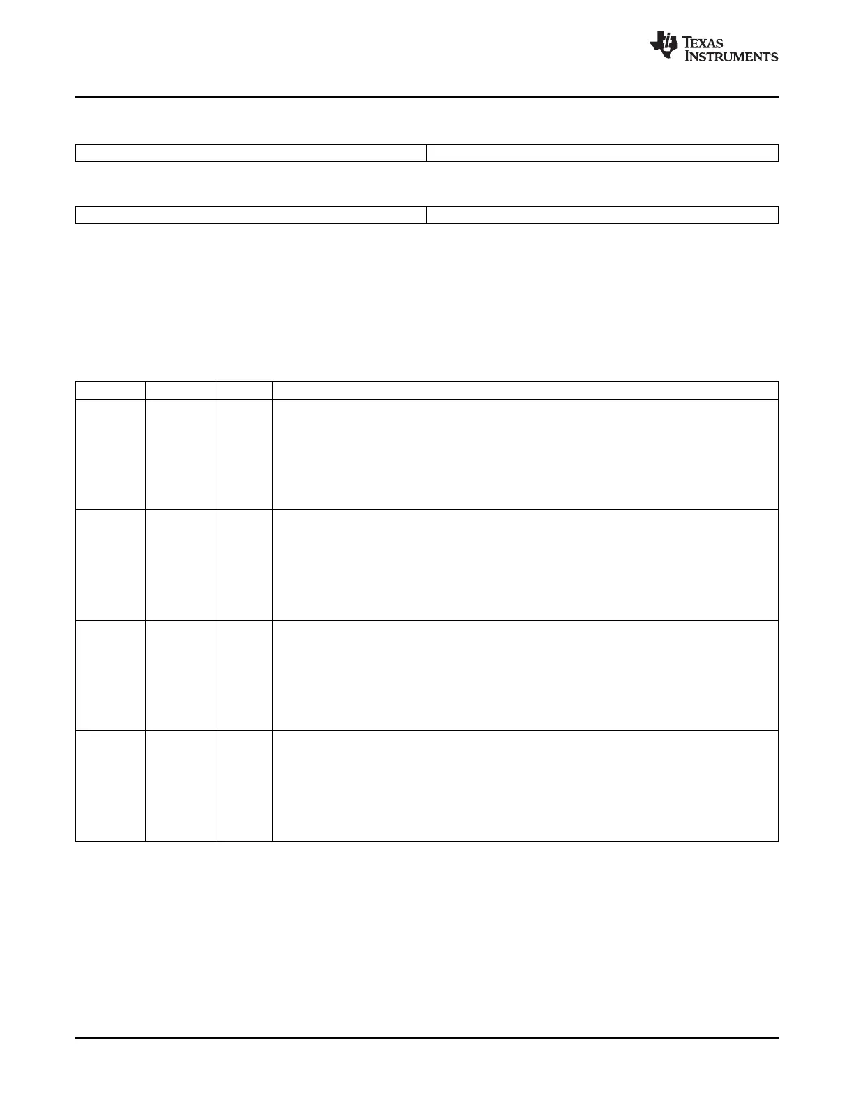
Figure 4-14. GPIO Port A Qualification Control (GPACTRL) Register
31 24 23 16
QUALPRD3 QUALPRD2
R/W-0 R/W-0
15 8 7 0
QUALPRD1 QUALPRD0
R/W-0 R/W-0
LEGEND: R/W = Read/Write; R = Read only; - n = value after reset
The GPxCTRL registers specify the sampling period for input pins when configured for input qualification
using a window of 3 or 6 samples. The sampling period is the amount of time between qualification
samples relative to the period of SYSCLKOUT. The number of samples is specified in the GPxQSELn
registers.
Table 4-18. GPIO Port A Qualification Control (GPACTRL) Register Field Descriptions
Bits Field Value Description
(1)
31-24 QUALPRD3 Specifies the sampling period for pins GPIO24 to GPIO31.
0x00 Sampling Period = T
SYSCLKOUT
(2)
0x01 Sampling Period = 2 × T
SYSCLKOUT
0x02 Sampling Period = 4 × T
SYSCLKOUT
. . . . . .
0xFF Sampling Period = 510 × T
SYSCLKOUT
23-16 QUALPRD2 Specifies the sampling period for pins GPIO16 to GPIO23.
0x00 Sampling Period = T
SYSCLKOUT
(2)
0x01 Sampling Period = 2 × T
SYSCLKOUT
0x02 Sampling Period = 4 × T
SYSCLKOUT
. . . . . .
0xFF Sampling Period = 510 × T
SYSCLKOUT
15-8 QUALPRD1 Specifies the sampling period for pins GPIO8 to GPIO15.
0x00 Sampling Period = T
SYSCLKOUT
(2)
0x01 Sampling Period = 2 × T
SYSCLKOUT
0x02 Sampling Period = 4 × T
SYSCLKOUT
. . . . . .
0xFF Sampling Period = 510 × T
SYSCLKOUT
7-0 QUALPRD0 Specifies the sampling period for pins GPIO0 to GPIO7.
0x00 Sampling Period = T
SYSCLKOUT
(2)
0x01 Sampling Period = 2 × T
SYSCLKOUT
0x02 Sampling Period = 4 × T
SYSCLKOUT
. . . . . .
0xFF Sampling Period = 510 × T
SYSCLKOUT
(1)
This register is EALLOW protected. See Section 5.2 for more information.
(2)
T
SYSCLKOUT
indicates the period of SYSCLKOUT.
General-Purpose Input/Output (GPIO)94 SPRUFB0C – September 2007 – Revised May 2009
Submit Documentation Feedback
 Loading...